Novel self-assembly can tune the electronic properties of graphene

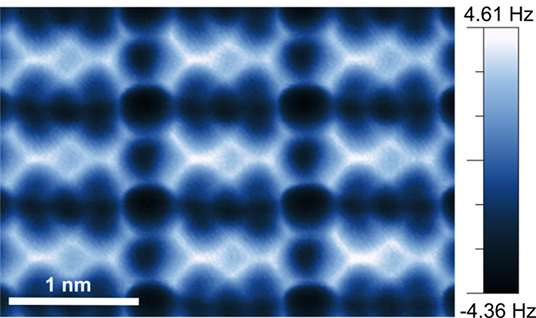
In what could prove to be a significant advance in fabricating new technologies, scientists discovered a new self-assembly mechanism that surprisingly drives negatively charged molecules to clump together to form islands when graphene is supported by an electrical insulator. Under these conditions, different charge interactions are not diminished, as they are when graphene is supported by a metallic substrate. At low concentrations, individual adsorbed molecules repel each other, but with increasing concentration, the molecules form two-dimensional islands. It was determined by theory that the flow of extra electrons into the islands from graphene keeps the molecules together. The electronic driving forces and stabilization energies are sufficient to overcome the repulsion between the negative charges.
This self-assembly mechanism can be used to tune the electronic properties of graphene layers in devices and control how electrons flow through the graphene. This mechanism permits atomic-scale patterning of electronic properties, which cannot be achieved with conventional lithographic techniques currently being used in the semiconductor industry.
Silicon has been successful because it is an electronically tunable semiconductor material that can be used in electronic devices. Graphene has distinct advantages over silicon for many applications due to its higher electron mobility and a very stable crystal structure, but it can be difficult to precisely tune. One way to tune the electronic properties of graphene is to adsorb molecules onto its surface. For example, negatively charged molecules on a graphene surface pull electrons from the graphene layer, changing its electronic properties. However, efforts to controllably assemble such negatively charged molecules have been limited because negatively charged species repel each other. Now scientists led by the University of California-Berkeley and Lawrence Berkeley National Laboratory have discovered that this repulsion can be overcome and two-dimensional islands can be controllably formed by negatively charged molecules on graphene supported by an insulator. Through microscopy and theoretical modeling, they determined that the underlying insulator was key to altering the nature of the interactions between the negatively charged molecules and graphene. These molecules are known to extract electrons from its substrate. At low surface concentrations, the negatively charged molecules separately accept electrons from the underlying graphene and repel each other, as expected because like charges repel each other.
Remarkably and counterintuitively, at higher concentrations, these charged molecules clump together to form ordered islands. This usual behavior is explained by theory as the donation of extra electrons to the islands of molecules by the graphene when compared to the donation to a single molecule. This extra charge makes it energetically more favorable to form islands. Surprisingly, this behavior observed on graphene substrate supported by an insulator does not occur when graphene is supported by a metal. This molecular self-assembly provides a possible alternative to patterning graphene using conventional lithographic techniques. Atomic-scale tuning of the properties of graphene layers could enable the fabrication of new devices based on graphene that cannot be made using silicon.
More information: Hsin-Zon Tsai et al. Molecular Self-Assembly in a Poorly Screened Environment: FTCNQ on Graphene/BN, ACS Nano (2015). DOI: 10.1021/acsnano.5b05322
Journal information: ACS Nano
Provided by US Department of Energy


