Taking microelectronics research to the atomic size future and beyond

At the IBM T.J. Watson Research Center in Yorktown Heights, N.Y., tucked between office desks and meeting rooms, there is approximately 40,000 square feet of cleanroom space which comprises the Microelectronics Research Lab (MRL). These cleanrooms consist of highly sophisticated tools run by a skilled team of engineers and scientists who spend their days processing silicon wafer after silicon wafer, and fabricating them into transistors and semiconductor devices, which are the brains of integrated circuits. To put this into perspective, the latest smartphones have billions of these tiny transistors inside just one of them.
Yet, teams of scientists at IBM Research are not fabricating these transistors for today's smartphones. Rather, they have their eye well on the future – busy experimenting with prototypes of next generation computing chips and devices. Today their research is focused on pushing the limits of silicon technology and Moore's Law, including the development of next generation logic and memory devices for scaling conventional computing devices to the 7nm node and beyond, as well as the fabrication of new cognitive and quantum solutions that will be the future of computing systems.
In fact, most recently, the 5-qubit device that is part of the IBM Quantum Experience was fabricated right in the IBM Research MRL. Creating new technologies like quantum computing is the goal of IBM's MRL and in order to develop new devices based on these technologies, researchers need highly advanced capabilities.
One example of the advanced facilities in the MRL is a semiconductor process tool from Tokyo Electron Limited (TEL) which provides unique plasma etching capability. This tool develops the processes needed to pattern and evaluate new devices and architectures consisting of a wide range of complex materials including III-V, carbon nanotubes and novel magnetic materials for non-volatile spin-transfer torque MRAM technology.
The steps to fabricating these new types of structures starts by loading silicon wafers into the process tool. Even though many new devices made of novel materials like carbon nanotubes or graphene, are introduced, all of them are built on a silicon foundation. Cleanroom conditions require scientists to wear overalls or "bunny suits" that cover most of their body to prevent any risk of contamination to the wafers from dust or oil. Robotic arms move the wafers from the loading chamber into the plasma chamber where they are processed using controlled gases and power, under ultra-high vacuum conditions. This is done by exposure of the wafer to the plasma phase. Before this stage the wafers are only patterned by lithography which will become permanent after exposure inside the plasma reactor.
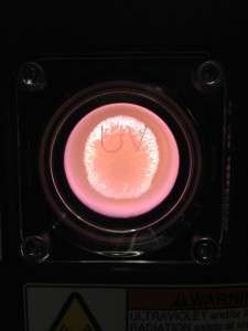
What happens during the plasma phase? According to Sebastian Engelmann, manager of the Advanced Plasma Processing Group at IBM Research, "Essentially this means the researchers light a plasma 'fire' in the reactor, which often glows like a flame and 'burns' the original pattern into the wafer. However, the key feature of this novel plasma source is that it burns off material without leaving any ashes."
Over the years, the team's work has gone from the micro level to the nano level, following the trend of miniaturization. As a result, the etching process has had to reach atomic scale dimensions, and today the team is developing new atomic layer etching (ALE) techniques. "As we scale our technologies and move toward advanced structures and devices, the level of precision one needs when etching into silicon substrates has to be extremely high," said Eric Joseph, senior manager and advanced materials and unit process technology research scientist at IBM. "We have to etch material and stop with angstrom-level precision."
To put it into perspective, when a car brakes it doesn't stop immediately when the brake pedal is depressed. It takes a certain distance before the car comes to a complete stop. The performance of a set of brakes on a car is the measurement of distance it takes to slow down and stop. "When it comes to etching new devices we need to stop on a dime and consume no more materials. This is incredibly important for carbon nanotubes, graphene and 2D materials, as their own thickness is in the region of two to three angstroms," Joseph said.
ALE offers the ability to etch (remove) one layer of atoms at a time from a substrate without disturbing or damaging the underlying layers or changing its properties. There are various approaches to ALE and the team at IBM Research has been exploring multiple methods, along with TEL and other partners, to achieve this capability for a variety of different material combinations.
In July, the IBM Research MRL will present their latest results at the 3rd International Workshop on Atomic Layer Etching, in Dublin, Ireland in which they explore one such promising approach incorporating electron beam generated plasmas. The work highlights the ability to enable ultra-high precision processing of atomically thin materials such as carbon nanotubes and/or graphene.
Provided by IBM


