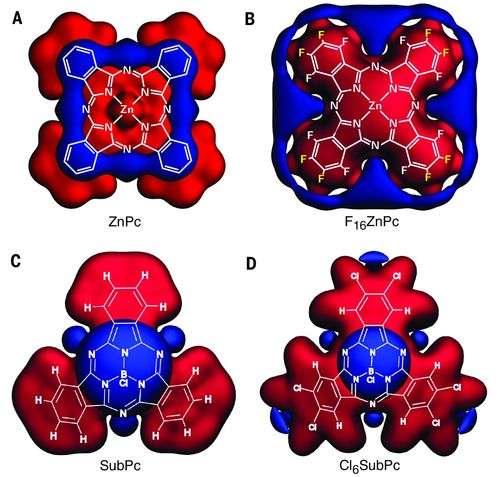
Molecular structural properties of (halogenated) ZnPc and SubPc. Credit: (c) Science (2016). DOI: 10.1126/science.aaf0590
(Phys.org)—A team of researchers with members from institutions in Germany and Switzerland has shown that band structure engineering is possible when designing organic semiconductors. In their paper published in the journal Science, the team describes a technique that involves long-range Coulomb interactions that are loosely bound by van der Walls forces. Nobuo Ueno with Chiba University, in Japan offers a deeper look at the work done by the team in a Perspective commentary in the same journal issue.
As Ueno notes, one of the most basic principles underlying semiconductor devices is the band gap—which is a measure of the energy needed to excite a material enough to make it conduct electricity. Much work has been done over the years to control the band gap in inorganic (non-carbon based) materials such as gallium, arsenide and of course silicon, by creating different alloys and putting them together in different ways to allow for tuning—success in this area meant that many different types of semiconductor based devices could be created. In recent years researchers have looked more and more at applying similar techniques to organic semiconductors, which as their name implies are semiconductors made from materials that are carbon based. Holding up such work has been an inability to find a way around the strong localization of the electronic states in them. In this new effort, the researchers report that they have developed a means at long last for engineering organic semiconductors.
The new approach involved taking note of the influence of Coulomb interactions (interactions that occur between electrically charged particles) which up to now, the team points out, have been mostly ignored by other researchers attempting to control band gaps in organic semiconductors. They found that the ionization energies of crystalline organic semiconductors could be tuned continuously over a large number of options by mixing them with their halogenated derivatives. In addition they showed that the photovoltaic gap and open-circuit voltage of organic solar cells could be tuned on a continuous basis by mixing the ratio of the donors.
As Ueno notes, this new technique could very well lead to the development of a whole new kind of device architecture—one that is able to take advantage of the ability to engineer the band gap in organic devices.
More information: M. Schwarze et al. Band structure engineering in organic semiconductors, Science (2016). DOI: 10.1126/science.aaf0590
Abstract
A key breakthrough in modern electronics was the introduction of band structure engineering, the design of almost arbitrary electronic potential structures by alloying different semiconductors to continuously tune the band gap and band-edge energies. Implementation of this approach in organic semiconductors has been hindered by strong localization of the electronic states in these materials. We show that the influence of so far largely ignored long-range Coulomb interactions provides a workaround. Photoelectron spectroscopy confirms that the ionization energies of crystalline organic semiconductors can be continuously tuned over a wide range by blending them with their halogenated derivatives. Correspondingly, the photovoltaic gap and open-circuit voltage of organic solar cells can be continuously tuned by the blending ratio of these donors.
Journal information: Science
© 2016 Tech Xplore


