UTA physicists use beams of antimatter to investigate advanced materials

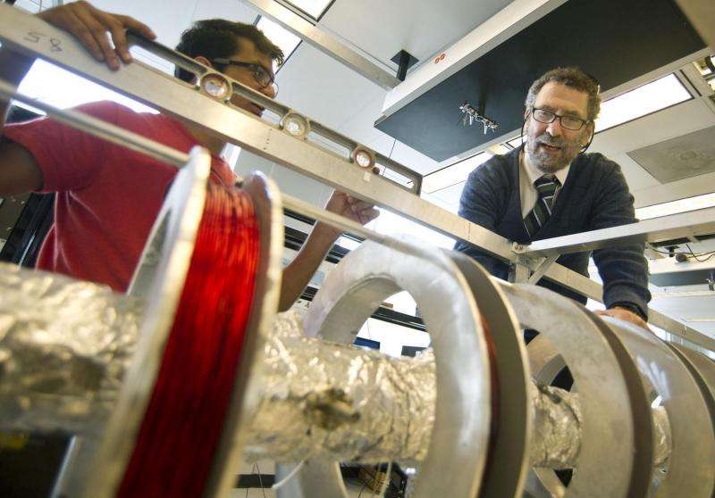
Researchers at The University of Texas at Arlington are developing a next generation positron beam facility that will enable them to analyze the properties of advanced materials for future electronics applications such as ultra compact high-speed computers and ultra small high-powered batteries.
Initial research is focusing on the characteristics of graphene, a versatile pure carbon material 200 times stronger than steel that is expected to provide ecologically-friendly, sustainable solutions across a huge variety of applications including electronics and biotechnology.
"Graphene is touted to be widely used in future applications like flexible electronics, organic LED and high-frequency transistors, " said Dr. Alex Weiss, a UTA Distinguished Professor of Physics, department chair and principal investigator of the project. "However, the exceptional properties of this material will only get translated into real-life applications when there is a proper understanding of the microscopic interaction of graphene at stable interfaces with other materials. Our research is supporting this area."
A $640,608 National Science Foundation Major Research Instrumentation Development Grant funded the project to build the enhanced beam and develop the UTA team's initial projects. UTA Physics professor Ali Koymen is co-principal investigator on the grant, which continues through 2016.
In their preliminary experiments, the UTA scientists used the new positron beam to explore the buried interface of eight layers of graphene on a copper substrate.
By implanting positively charged positrons on the graphene and graphene-copper interfaces, they could generate "annihilation" events with negatively charged electrons. These matter-antimatter "annihilations" produce electrons and gamma waves that carry information concerning the chemical nature, electronic structure and defects of the surfaces and interfaces at those sites.
The UTA researchers also combined two advanced positron spectroscopic techniques, a first in the world in their field, to improve the quality of their measurements.
The first technique is called Positron Annihilation Induced Auger Electron Spectroscopy, or PAES, which was invented by Dr. Weiss at UTA. This tool is considered unique among surface science techniques in being able to probe both chemical content and local electronic structure of the topmost atomic layer with an extremely high level of selectivity. The other was a well-established tool for studying defects in materials, known as coincidence Doppler broadening gamma spectroscopy.
"By combining their expertise and research experience, Dr. Weiss and his collaborators are building a materials characterization facility at UTA that is truly unique," said Duane Dimos, UTA vice president of research. "It will undoubtedly result in noteworthy advances in multiple areas."
The UTA group plans to further develop the facility in the next few years by adding the capability to make measurements of the magnetic properties of nanomaterials through the addition of spin polarization - a uniform alignment of the positrons' spin or magnetic positioning - as another unique feature to the UTA beam.
That feature will allow researchers to probe magnetic structures by determining their surface electrons' "spin state," Dr. Koymen said."Positrons are hundreds of times more likely to annihilate with an electron that is in the opposite spin state as opposed to a parallel spin state," he said. "The intensity of the upgraded beam will allow us to make this kind of difficult measurements in a reasonable time frame."
Additional potential areas for research aided by the upgraded positron beam include:
- Topological insulators, an emerging field of materials that act as insulators except for their surface, which is highly conductive. Researchers are exploring how their unique properties could lead to faster semiconductor chips for electronics.
- Tribology, the investigation of friction, lubrication and wear. Specifically, the beam can be used to examine the surface of soot particles to increase understanding of the abrasive behavior of soot in diesel engines.
- Defects in material surfaces: by measuring Doppler shift in the gamma rays to identify "lattice defects" that can degrade the performance of optical and electronic devices. The new positron beam system can save time and energy in carrying out high precision experiments.
Provided by University of Texas at Arlington


