Doping crystals of nanocrystals

Silicon semiconductors form the basis of all modern electronics and microprocessors. Crucial to these applications is the ability to 'dope' the semiconductor; which is to say, by controllably adding impurity atoms to a semiconductor, one can continuously vary its electronic and optical properties.
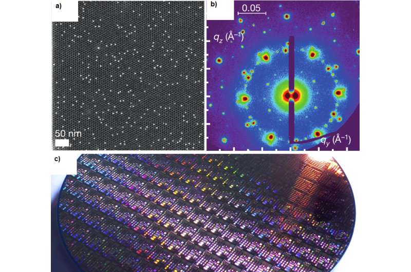
A recent collaboration of scientists from the University of Pennsylvania and NIST has demonstrated for the first time, a unique nanoscale analogue. In particular, nanoscale crystals are created by assembling nanoparticles into close-packed arrangements (so-called 'nanoparticle superlattices'). In this work, the assembly is performed with controlled amounts of 'impurity' nanoparticles that differ from those used to form the host crystal.
The resulting superlattices are 'doped', and exhibit properties that depend sensitively on the concentration and intrinsic behavior of the dopant particles. In one example, by controlling the concentration of doping gold nanoparticles (into a crystal of lead selenide nanoparticles), the conductivity could be tuned over 6 orders-of-magnitude.
To characterize the ordering in these nanomaterials, x-ray scattering measurements were performed at the X9 beamline (NSLS), which is co-managed by the CFN. This ability to rationally tune the properties of superlattices will be crucial to future applications of optical and electronic materials.
- The controllable introduction of dopant particles into well-defined nanoparticle superlattices, without disrupting the lattice crystallinity, is the first demonstration of specific tailoring the electronic transport properties of bulk nanoparticle ensembles.
- Gold nanoparticle doping enhanced the conductivity of lead selenide nanoparticle films by over 6 orders of magnitude.
- Such control over the introduction of nanoparticles into superlattices opens up possibilities for doping of other nanomaterials, such as magnetic and catalytic nanoparticles.
CFN's transmission small-angle x-ray scattering (TSAXS) endstation at the NSLS X9 x-ray beamline was used to measure the nanoparticle superlattice crystals.
More information: "Substitutional doping in nanocrystal superlattices." Nature 524, 450–453 (27 August 2015) DOI: 10.1038/nature14872
Journal information: Nature
Provided by Brookhaven National Laboratory


