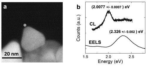
On the left, a STEM image of a triangular gold nanoparticle sitting on titanium oxide surface. The white circle at the top corner of the gold nanoparticle indicates where the electron beam is making spectroscopic measurements. On the right are the corresponding spectra representing electron absorption and emission. Credit: Sharma/NIST
A close-up view of an individual tree won't tell you much about what's going on in the forest, or even what's going on in the tree's upper branches. The same goes for studying nanoparticles. What is happening in one small area might not be indicative of what's going on with the nanoparticle as a whole. In fact, the light you shine on the area may actually affect the reaction processes, giving a skewed reading.
To correct for this experimental myopia, researchers at the National Institute of Standards and Technology (NIST) have developed a relatively simple setup that makes it possible for scientists to image simultaneously nanoscale features and microscale (nano x 1,000) chemical interactions. Their approach combines two powerful analysis tools: environmental scanning transmission electron microscopy (ESTEM)—a variation on traditional electron microscopes that enables researchers to view a specimen in a reactive environment,i.e., not in a vacuum—and Raman spectroscopy, which uses light interactions to identify molecular structures from their characteristic vibrations.
Having such a global view of nanoparticles would be useful to scientists working in a broad range of research areas from nanotechnology to pharmaceuticals and biotechnology.
The group used the technique during recent experiments to image carbon nanotubes as they germinated and grew on the surface of cobalt carbide nanoparticles.
Their description of the development of the new imaging setup appeared in the journal Ultramicroscopy.
The team's technique consists of inserting a parabolic mirror attached to a hollow rod below the sample they wish to study. The parabolic mirror serves two purposes. It focuses the light from a source such as a laser, outside the ESTEM, onto the sample and collects the sample's response to light excitation, i.e., Raman spectra for analysis.
Schematic view of the integrated optical spectroscopy system developed at NIST. The laser goes through the sapphire window, bounces off the parabolic mirror and onto the sample above. The parabolic mirror also collects a portion of the vibrational spectra/photons emitted by the sample for analysis. Credit: Sharma/NIST
The mirror also collects the light signals emitted when the sample is excited by the microscope's electron beam in the same area where atomic-scale images are being collected. For example, surface plasmons are highly localized electromagnetic waves that flow along a surface, and their glow is extremely sensitive to changes in that surface.
As a bonus, according to NIST researcher Renu Sharma, measuring the shifts in Raman signal energy also enables them to measure the temperature of a sample region, a capability that is currently not universally available.
"Most importantly, the ESTEM-Raman combination will provide us with the unique opportunity to study gas and temperature effects on technologically important nanostructures," says Sharma. "For example, the morphology or makeup of quantum structures may change as a function of temperature, environment and time, thus degrading its efficiency or lifetime. This can be revealed by simultaneous collection of in situ imaging and surface plasmon data."
While the technique was developed for use with an ESTEM, the vibrational and optical spectroscopy elements the group developed can be adapted for any transmission electron microscope column.
More information: M. Picher, S. Mazzucco, S. Blankenship, R. Sharma. "Vibrational and optical spectroscopies integrated with environmental transmission electron microscopy." Ultramicroscopy. Volume 150, March 2015, Pages 10–15. DOI: 10.1016/j.ultramic.2014.11.023
Provided by National Institute of Standards and Technology


