February 3, 2015 report
Research team succeeds in building transistors using silicene

(Phys.org) —A team of researchers with members from Italy and the U.S. has succeeded in building a transistor based on silicene, for the very first time. In their paper published in the journal Nature Nanotechnology, the team describes how they were able to get the notoriously finicky material to cooperate.
Silicene is where silicon is made in one atom-thick sheets—like graphene, it has proven to have fantastic electrical properties, which means it could be useful in future electronics, particularly as researchers continue to attempt to make faster or smaller computer chips. The problem with silicene is that it is very difficult to make and even more difficult to work with once a sheet is at hand. It has been only eight years since physicist Lok Lew Yan Voon published theories about how silicene would perform, and since then, various groups have tried creating the material, most finding little to no success. Those groups that have succeeded have found that getting the sheets to behave has been a serious hurdle to using it for any practical purposes. In this new effort, the researchers report that not only have they been able to create the material, but they have found a way to tame it enough to allow them to create tiny transistors.
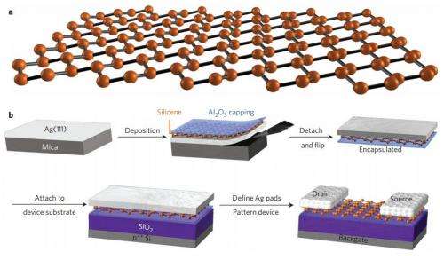
To get the nanosheets to cooperate the researchers first grew some sheets of it on a very slim base of silver that had been topped with aluminum oxide. Once grown, the silicene sheet was peeled off its base and placed silver side up on a silicon dioxide wafer. The silver was then fashioned to make electrical contacts allowing the sheet to be used as a transistor. The team reports that they built several such transistors and that they were stable when used in a vacuum. They also report, that thus far, the performance of the silicene has lived up to the theories that predicted its properties.
Though the team has technically created a transistor based on silicene, it is still not clear if such a process would be amendable to porting to a commercial application. Much more research will have to be done before that is determined. If it does work out, the team believes it would be easier to use silicene in future electronics than graphene, because so much of chip design is already silicon based.
More information: Silicene field-effect transistors operating at room temperature, Nature Nanotechnology (2015) DOI: 10.1038/nnano.2014.325
Abstract
Free-standing silicene, a silicon analogue of graphene, has a buckled honeycomb lattice1 and, because of its Dirac bandstructure2, 3 combined with its sensitive surface, offers the potential for a widely tunable two-dimensional monolayer, where external fields and interface interactions can be exploited to influence fundamental properties such as bandgap4 and band character5 for future nanoelectronic devices6, 7. The quantum spin Hall effect3, chiral superconductivity8, giant magnetoresistance9 and various exotic field-dependent states7 have been predicted in monolayer silicene. Despite recent progress regarding the epitaxial synthesis of silicene8, 9, 10 and investigation of its electronic properties11, 13, 14, 15, to date there has been no report of experimental silicene devices because of its air stability issue16. Here, we report a silicene field-effect transistor, corroborating theoretical expectations regarding its ambipolar Dirac charge transport17, with a measured room-temperature mobility of ∼100 cm2 V–1 s–1 attributed to acoustic phonon-limited transport18 and grain boundary scattering. These results are enabled by a growth–transfer–fabrication process that we have devised—silicene encapsulated delamination with native electrodes. This approach addresses a major challenge for material preservation of silicene during transfer and device fabrication and is applicable to other air-sensitive two-dimensional materials such as germanene2, 3, 4 and phosphorene19, 20. Silicene's allotropic affinity with bulk silicon and its low-temperature synthesis compared with graphene or alternative two-dimensional semiconductors suggest a more direct integration with ubiquitous semiconductor technology.
Journal information: Nature Nanotechnology
© 2015 Phys.org


