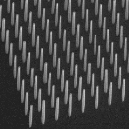
Scanning electron microscope image of an array of GaN nanowires with a spacing of 800 nm.
Defect-free nanowires with diameters in the range of 100 nanometers (nm) hold significant promise for numerous in-demand applications including printable transistors for flexible electronics, high-efficiency light-emitting diodes, resonator-based mass sensors, and integrated, near-field optoelectronic tips for advanced scanning tip microscopy.
That promise cannot be realized, however, unless the wires can be fabricated in large uniform arrays using methods compatible with high-volume manufacture. To date, that has not been possible for arbitrary spacings in ultra-high vacuum growth.
Now NIST's PML's Optoelectronic Manufacturing Group has achieved a breakthrough: Reproducible synthesis of gallium-nitride nanowires with controlled size and location on silicon substrates.
The result was achieved by improving selective wire-growth processes to produce one nanowire of controlled diameter per mask-grid opening over a range of diameters from 100 nm to 200 nm. Ordered arrays with a variety of spacings were fabricated.
In the near term, the research will be used to create a wafer-scale arrays of probes for devices that examine the surface and near-surface properties of materials, to optimize nanowire LEDs, and to produce nanowires with controlled diameter for a collaborative project involving printable transistors for millimeter-wave reconfigurable antennae.
Provided by National Institute of Standards and Technology


