Reimagining silicon

Silicon (Si) is ubiquitous in modern semiconductor manufacturing. Well-established procedures for its processing, perfected over more than five decades of industrial use, enable a diverse array of electronic devices that pervade everyday life. The highly evolved supply chain that accompanies Si's dominance also enables very low manufacturing costs. In fact, it is far cheaper to fabricate a Si-based transistor than print a single letter in a newspaper.
The specific form of Si that fuels the ongoing semiconductor revolution is known as "diamond cubic." This particular structure – the arrangement of atoms – readily forms during traditional processing. It is this structure that imparts Si with the properties that have been exploited in devices ranging from integrated circuits to solar cells. Importantly, because the properties of bulk diamond cubic Si are fixed, most think its long-term usefulness is limited. Yet this narrow view of a material's capabilities, Si or otherwise, and thus its utility in specific applications, assumes that rearranging the atoms into new structures is exceedingly difficult or impossible.
What if techniques were available to program alternative structures? What new properties would arise? What applications might these reimagined materials enable? Dr. Michael A. Filler, an assistant professor in the School of Chemical & Biomolecular Engineering, and his research group are asking these questions about nanomaterials in general, and Si nanowires in particular.
The promise of designing materials with entirely programmable atomic arrangements, specifically the extensive property tunability that would accompany it, is what motivates his research team. "Such a capability would allow us to rethink the structure of new and old materials alike, so that they can conduct electricity, transport heat, or absorb light in distinct ways," Filler says.
Filler's research is inspired by the work of organic chemists, who apply a suite of synthetic methods, born from a basic knowledge of chemical bond breaking and forming, to create remarkably intricate functional molecules. "But unlike organic chemistry, the synthesis of most nanoscale materials is poorly understood, cannot be adequately controlled, and, as a result, yield low quality materials," comments Filler.
Researchers frequently probe a material only after it has been made and, consequently, are unable to retrieve detailed information about the synthesis itself. "We watch the synthesis while it's taking place," Filler says." Once we have a better understanding of what's going on, we can precisely engineer the structure we want."
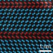
Filler and his graduate student Naechul Shin recently showed for the first time that the stacking of atoms in a Si nanowire could be rationally manipulated. To do this, they controlled when and where special "structure directing" species attached to and covered the nanowire surface. This molecular coating forced the next layer of Si atoms to position themselves differently from the prior layer. "The rapid addition and removal of these species, whose chemical signatures we can observe in real time, allowed us to control the arrangement of Si atoms in the nanowire from one layer to the next," says Filler. His group continues to refine their approach and will begin testing the properties of this new form of Si in the near future. Filler foresees that this work will find use in fields ranging from electronics and photonics to energy conversion and catalysis.
However, directing individual layers of Si atoms is just the first step, and as science and research continue to advance, Filler says there will be much more control over atomic placement in many materials. "The chemical engineers and materials scientists of the future will be able to choose the placement of every atom in a material," says Filler.
Provided by Georgia Institute of Technology


