May 22, 2014 report
Researchers find a way to integrate two two-dimensional materials into a single electronic device

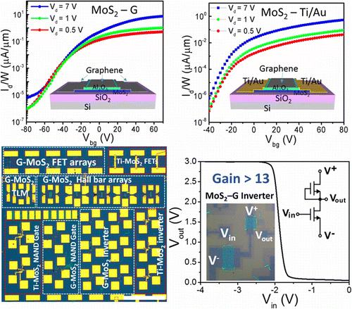
(Phys.org) —Researchers working at the Massachusetts Institute of Technology have found a way to integrate two different two-dimensional materials in one single electronic device. In their paper published in the journal Nano Letters, the team describes how they used both graphene and molybdenum disulfide (MoS2) to create a single circuit.
Two dimensional materials (so named because they are just one atom thick) have created a lot of buzz in the electronics community because of their unique electronic properties. Scientists hope to use them to create smaller, more efficient devices. The two main materials that have captured the attention of the research world are graphene (a sheet of carbon) and MoS2. Both have shown promise, but each has its limitations. To take advantage of what each does well, and to avoid the disadvantages, researchers have looked to joining the two on a single circuit. In this new effort the team at MIT is reporting that they've done just that, creating large-scale electronic circuits.
Getting the two materials to cooperate was no easy feat. They started by growing samples of MoS2 and graphene using chemical vapor deposition. The MoS2 was then etched to fashion it into channels, followed by a process that caused aluminum oxide (Al2O3) to form on its surface. Graphene sheets were then applied to the channel, cut with oxygen plasma to form gate electrodes and source drains. In the final result, the Al2O3 serves to protect the MoS2 allowing the circuit to run as designed.
The researchers believe their fabrication process could be used to allow for integrating many types of two-dimensional materials, allowing for the creation of whole new device types, e.g. lasers, tunneling microscopes and a variety of transistors. An additional plus, they note, is that because the finished products are exceptionally thin, they can be bent to allow for the creation of circuits of virtually any shape. The circuits are also transparent, which means they could likely be used for new types of personal technology devices (skin patches or those that can be sewn into clothes, for example) or as a part of hidden sensors. The team plans to next work on integrating insulating layers onto their tiny circuits, allowing for the creation of even more exotic circuitry.
More information: Graphene/MoS2 Hybrid Technology for Large-Scale Two-Dimensional Electronics, Nano Lett., Article ASAP. DOI: 10.1021/nl404795z
Abstract
Two-dimensional (2D) materials have generated great interest in the past few years as a new toolbox for electronics. This family of materials includes, among others, metallic graphene, semiconducting transition metal dichalcogenides (such as MoS2), and insulating boron nitride. These materials and their heterostructures offer excellent mechanical flexibility, optical transparency, and favorable transport properties for realizing electronic, sensing, and optical systems on arbitrary surfaces. In this paper, we demonstrate a novel technology for constructing large-scale electronic systems based on graphene/molybdenum disulfide (MoS2) heterostructures grown by chemical vapor deposition. We have fabricated high-performance devices and circuits based on this heterostructure, where MoS2 is used as the transistor channel and graphene as contact electrodes and circuit interconnects. We provide a systematic comparison of the graphene/MoS2 heterojunction contact to more traditional MoS2-metal junctions, as well as a theoretical investigation, using density functional theory, of the origin of the Schottky barrier height. The tunability of the graphene work function with electrostatic doping significantly improves the ohmic contact to MoS2. These high-performance large-scale devices and circuits based on this 2D heterostructure pave the way for practical flexible transparent electronics.
Journal information: Nano Letters
© 2014 Phys.org


