Design of optical modulators with low losses to improve optical communications

Modulators are key components within optical fiber networks and serve to transfer information from an electrical current to a signal suitable for optical fibers. They function by turning a light beam on and off quickly and the faster they can do this, the more data that can be transmitted.
An increase in data traffic creates a need for a reduction in the cost and size of optical components. An improved low-loss design for modulators, suitable for silicon computer chips, has been developed by Soon Thor Lim and colleagues from the A*STAR Institute of High Performance Computing, the A*STAR Institute of Microelectronics and collaborators from Fujikura Ltd.
Existing optical modulators are based on lithium niobate, a material that is expensive and unsuitable for silicon chips. While silicon offers an inexpensive alternative, it can only be used with the addition of other elements that can create positive and negative movable electrical charges. Modulation requires the movable charges to be channeled in and out of the device by an alternating electrical voltage, which controls both the speed of light through the chip and the data rate. Light that passes through this region and crosses light that passes through a neutral silicon region creates interference effects in the optical beam that switches the light on and off.
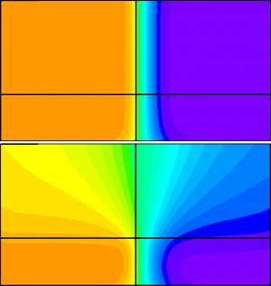
Previous modulator designs contained charged regions that were relatively large, with the drawback that they increased light absorption in the chip. However, in the team's proposed design, this area is reduced so that less of the laser beam passes through the charged region (see image).
After computer modeling the performance of the modulator, the team fabricated their device on a silicon chip that has light channels only 220 nanometers high and 550 nanometers wide. Compared to designs with large charged areas, these modulators reduced optical losses by up to 28 per cent and operated at faster speeds of 10 gigabits per second.
"Our device has a speed and optical losses comparable to existing technology such as lithium niobate," says Lim. "One reason for this high performance is because we used highly accurate computer codes developed in-house."
Successfully demonstrating the device also highlights how modeling software can reduce the required number of experiments, Lim adds. "Simulation and analysis helps to visualize the physical behavior of these cutting-edge optical devices. This can identify potential problems and circumvent the need for costly multiple design iterations ultimately accelerating the speed to market."
More information: Goi, K., Ogawa, K., Tan, Y. T., Dixit, V., Lim, S. T. et al. Silicon Mach–Zehnder modulator using low-loss phase shifter with bottom PN junction formed by restricted-depth doping. IEICE Electronics Express 10, 20130552 (2013). dx.doi.org/10.1587/elex.10.20130552


