Novel microfluidic material breakthrough for wafer-scale mass production of lab-on-chip

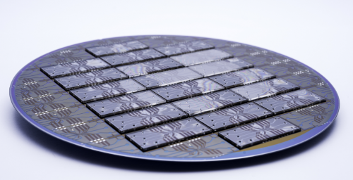
Imec, a world-leading nanoelectronics research center and JSR, a leading materials company, announce that they have successfully used JSR's innovative PA (Photo-patternable Adhesive) material for wafer-scale processing of lab-on-chip devices. With PA as a key enabling material, imec has processed microfluidic cell-sorter devices, merging microheaters and sensors with wafer-scale polymer microfluidics. PA is a breakthrough material: a good microfluidic channel material and adhesive at the same time, suitable for wafer-scale processes and mass production.
Lab-on-chip technology will drive a revolution in medical technology in the years to come. It will enable powerful point-of-care diagnosis and treatment through on-chip molecular synthesis, separation, sensing, and detection. Key will be the ability to integrate microfluidics with heterogeneous components such as electronics, sensors, microheaters, and photonics in a cost-effective manner. To merge these elements successfully, new bonding and surface treatment materials are needed.
"PA solves a number of issues that we have with other materials, such as the widely-used PDMS (polydimethylsiloxane, a silicon-based organic polymer)", says Liesbet Lagae, imec R&D manager of life science technologies. It has all the characteristics we are looking for in a photopatternable material to create microfluidic channels on silicon wafers, including a good channel definition and biocompatibility. But at the same time, it is an adhesive that allows direct thermal bonding with the cover glass. And unlike PDMS, it allows for wafer-scale processing, which is a prerequisite for industrial mass production."
Imec used PA to process the next generation of its cell sorter lab-on-chip. Integrating on-chip imaging, in-flow cell tomography to identify cells, and bubble jet-flow technology to guide and sort individual cells, the prototype lab-on-chip can process up to 2,000 cells per second. One application envisaged for these ultrafast cell-sorters is the detection of circulating tumor cells in human blood.
JSR and imec are longstanding partners in the development of semiconductor technology and materials going back to the late 80's. JSR has taken a great interest in microfluidics materials, which it started developing in partnership with imec starting 2011. Two years of R&D including the assessment of biocompatibility and process compatibility have now resulted in a material solution for lab-on-chips such as imec's cell sorter. Luc Van den hove, CEO of imec: "JSR has now also become a key material supplier in the life science ecosystem. Together, JSR and imec will continue to develop material solutions for life science applications."
"Most applications face the challenge of selecting the right materials and technologies," emphasizes JSR's CEO Nobu Koshiba. "Our collaboration with imec proves that open-innovation is key to move from early-stage precompetitive technology to the development of robust products such as these next-generation medical devices."
Provided by IMEC


