November 5, 2013 feature
Better, faster, simpler: Depositing graphene directly onto flexible substrates

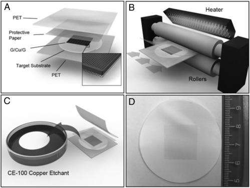
(Phys.org) —The wunderkind material graphene is a one-atom thick layer of graphite (another crystalline form of carbon) in which carbon atoms are arranged in a regular hexagonal pattern. Being very strong, light, nearly transparent, and an excellent conductor of heat and electricity, is finding new applications at a dizzying rate. This is not surprising, given that its myriad characteristics include its electronic, optical, excitonic, thermal, spin transport, anomalous quantum Hall effect, mechanical, and other unique properties. Although one of graphene's attractive mechanical properties is its flexibility, most research into those properties has been conducted on rigid substrates such as silicon dioxide or quartz. A rigid substrate is suitable for transistors or photoelectric devices, but applying graphene to flexible substrates has numerous applications, such as organic electronics (used in solar cells, light-emitting diodes, touch screen technology, photodetectors, and molecular separation membranes), photonics, and optoelectronics. Currently, there's little reported activity in transferring graphene onto flexible substrates, and these typically use polymethylmethacrylate (PMMA) as an intermediate membrane – the downside being that the membrane must be removed after the transfer. Recently, however, scientists at MIT, University of Alabama and Universidade Federal de Minas Gerais devised a simple, PMMA-free, direct lamination technique for transferring graphene onto various flexible substrates. While their direct transfer method doesn't work on hydrophilic substrates like paper or cloth, the new technique also can work successfully in these works by using PMMA as a surface modifier or adhesive – a capability that they say will create opportunities for ubiquitous or wearable electronics.
Prof. Paulo T. Araujo and Prof. Jing Kong discussed the research that their students, Luiz Gustavo Pimenta and Yi Song, and colleagues conducted in an interview with Phys.org. "The concept behind the lamination technique is simple and, as one can see in our paper's references, we were not the first ones to apply it," Araujo tells Phys.org. "However, we were the first ones to apply it in a very clean way – that is, without help of intermediate membranes such as PMMA, or glues such as thermal tapes." The main challenges they encountered, he notes, were optimizing parameters like lamination machine temperature, and fabricating the appropriate layered composition of the target substrates, graphene, copper foil, and protective pellicles. "Additionally," Araujo adds, "we needed to understand the differences and similarities among the substrates we used. For example, a very porous substrate requires a different transference strategy from which is very smooth."
Araujo notes that the new transfer method specifically contrasts with previous methods in terms of speed and simplicity. "In short, the most used transfer method consists of spincoating PMMA over a cooper foil with graphene grown on it. After that, the cooper/graphene/PMMA set is left in a cooper etchant for 30 minutes, which eliminates the cooper, leaving only the graphene/PMMA survives. Next, we rinse the graphene/PMMA set with DI water and finish it with the target substrate. Finally, acetone or annealing is used to get rid of the PMMA. The entire process takes approximately 1-1.5 hours." The new direct transfer method eliminates most of the above steps, except those involving the cooper etchant and the cleaning with DI water. "Therefore," he adds, "I'd say that direct transfer saves approximately half an hour."
Araujo points out that a key factor was identifying the important factors needed for a successful transfer onto bare substrates. "The first step was to identify differences and similarities among the substrates we used, or that could be used, in our research – namely, if porous/non-porous, hydrophobic/hydrophilic, soft/hard, behavior of under temperature variation, and so on. Then, through a careful and methodical plan, we had to exclude those differences/similarities which did not play any role in the transfer." This step was particularly laborious, Araujo says, because it involved multiple direct-transfer experiments carried under the extremely varied conditions. As a result of this effort, the scientists concluded that the most important target substrate factors were its hydrophobicity and contact area with the graphene/copper set.

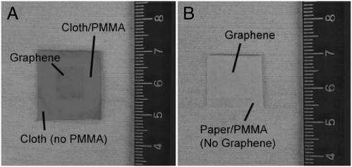
As to substrates not suitable for a direct transfer, the team also determined that PMMA can be used either as a surface modifier or as a glue to ensure a successful graphene transfer. "First, we needed to see if our hydrophobicity prediction was correct – and PMMA was a very convenient choice, since it's hydrophobic," Araujo explains, "and. hydrophobic substrates worked very well for the transfer. We therefore asked if we could turn a hydrophilic substrate, with which the transfer had previously failed, into one that is hydrophobic substrate." The answer was yes – and we can could use PMMA, since it is soft (meaning that they it could potentially achieve the needed glass temperature transition) and hydrophobic. "However," he adds," this led us to another question: If we spincoat PMMA over the hydrophilic substrate, will the transfer work?" Testing showed that it did, enabling graphene transfer onto cloth and paper.
Regarding the team's demonstration that multilayers enable large area conducting sheets to be placed on most substrates they studied, Kong acknowledges this step was straightforward from the point of view of direct transfer. "Since graphene is hydrophobic, and assuming that the first transfer was successful, we could perform multiple transfers successfully," he points out. "The hardest part was capturing scanning electron microscope images of multiple-graphenes over the flexible substrates. Being insulators, the substrates get electrically charged very easily, which prevented us from seeing the substrate/graphene set. Also, sheet resistance measurements were tricky, since the fragile substrates are very often damaged by the probes."
In addressing these challenges, Araujo says that the key insight came from thinking about the critical factors in the interaction between graphene and PMMA/thermal tapes. "The great innovation was certainly to show that, for most commercial substrates, we do not need to use any intermediate membrane to transfer graphene to the flexible substrates. The absence of the intermediate membranes provides a clean transfer which greatly improves the quality of the transferred material. Finally, in my point of view, it's fantastic to show that we can transfer graphene onto cloth or paper by treating then with a PMMA membrane which offers the environment necessary to make the transfer work – a method can easily be described as a new technique to transfer graphene into this class of substrates."
In the near future, Kong says that there will be a strong need for alternative ways of harvesting energy. "In this context," she explains, "the ability to adequately synthesize and manipulate and transfer relevant materials from the growth station to the target platforms is a major problem, since these steps will determine the quality of the final product. The growth of graphene is already quite advanced – and what we're offering with this research is a simple recipe to make multiple transfers of materials while avoiding contaminants brought along with standard 'glue-based' procedures."
Araujo sees this advance leading to a new era of high quality flexible touch screens, flexible light emitting diodes, flexible sensors, gas filters and solar cells. Furthermore, he notes that with the emergent interest in new layered materials – for example, boron nitride, transition metal dichalcogenides, and oxides – it will become possible to fabricate heterostructures by intercalating different materials. "The different ways in which one intercalates the layered materials provide a whole new class of applications involving electronics, spintronics, superconductivity and optoelectronics," Araujo says, adding that the residue-free transfer procedure might also represent an advance to building high-quality heterostructures.
"In terms of the planned next steps in our research," Kong continues, "the extension of our methodology should be tested with other layered materials such, including the boron nitride, transition metal dichalcogenides and oxides those mentioned above as well as other substrates. A more thorough study regarding the temperatures determining the hot/cold transfer should be conducted as well."
Another challenge Araujo cites is the structural quality of the transferred material. "Even though we've demonstrated the residue-free transfer concept and addressed reasons for a successful transfer, the continuity of the transferred film is still not at state-of-the-art. The lack of continuity is welcome for some applications, such as filters – but it's undesirable in the production of, for example, high-quality touch screen devices. Also," he concludes," the extension of this technique to perform this residue-free transfer to rigid substrates is still a challenge – and it's worth remembering that even though the technological appeal of flexible devices is high, many applications involving, for example, logic circuits, are still strongly connected to rigid substrates."
More information: Direct transfer of graphene onto flexible substrates, PNAS Published online before print October 14, 2013, doi:10.1073/pnas.1306508110
Journal information: Proceedings of the National Academy of Sciences
© 2013 Phys.org. All rights reserved.


