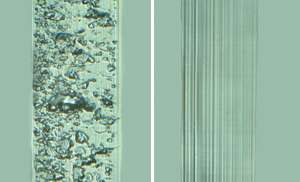
New and verified computer model improves machining of nanoscale semiconductor parts for the electronics industry

Brittle materials such as silicon and ceramics are used extensively in the semiconductor industry to make component parts. Materials cut to have a mirror-like surface yield the best performance, but the precision required is difficult to achieve at such a tiny scale.
Xinquan Zhang at A*STAR's Singapore Institute of Manufacturing Technology, along with co-workers at the same institute and the National University of Singapore, has developed a computer model that allows engineers to predict the best way of cutting different materials using vibration-assisted machining (VAM). This technique periodically interrupts the cutting process via the application of small-amplitude and high-frequency displacement to the cutting tool.
"Many researchers have observed that using VAM instead of conventional cutting techniques allows them to make cleaner, fracture-free cuts to most brittle materials," explains Zhang. "Because no theory or model exists to explain or predict this phenomenon, we decided to investigate."
At the nanoscale, brittle materials exhibit a certain degree of plasticity. Each material has a particular depth of cut that allows clean shearing to occur without chipping or fracturing on, or beneath, its surface. This point, known as the critical undeformed chip thickness, is directly correlated with material properties and machining conditions.
Zhang and his team studied the behavior of different brittle materials cut with VAM, during which two modes of cutting occur. In the ductile mode, plastic deformation caused by cutting is followed by elastic rebound and recovery of the material structure between vibrations. The brittle mode, on the other hand, removes material by uncontrolled crack propagation. Making a clean cut during ductile mode—before the brittle mode dominates—is therefore desirable.
The researchers modeled the energy consumption of each mode in terms of material removal as the vibrating tool moved, taking into account tool geometry, material properties and the cutting speed.
"By examining energy consumption and material deformation we were able to describe the mechanics when VAM moved from the ductile to the brittle mode," explains Zhang. "We then established a model to predict [the] critical undeformed chip thicknesses by finding the transition point between the two modes."
Through a series of experiments, the team verified that the model accurately predicts the critical undeformed chip thicknesses of single-crystal silicon when cut at various VAM speeds.
"Our model will help engineers to select optimized machining parameters depending on their desired material," says Zhang. "Advantages could include higher productivity, lower costs, and improved product quality for semiconductor parts and other nanoscale technologies."
More information: Zhang, X., et al. Amodel to predict the critical undeformed chip thickness in vibration-assisted machining of brittle materials, International Journal of Machine Tools and Manufacture 69, 57–66 (2013). dx.doi.org/10.1016/j.ijmachtools.2013.03.006


