September 13, 2013 report
Defects in 2D semiconductors could lead to multi-colored light-emitting devices

When scientists remove individual atoms in a semiconductor material, the resulting vacancies become point defects. Contrary to what their name implies, these defects can have beneficial effects on the semiconductor's properties and enable most functionalities of electronic materials. In a new study, researchers have demonstrated that point defects in 2D semiconductors result in an increase in the overall room-temperature photoluminescence intensity. Further, the defects create a new emission peak that could lead to a better understanding of defect physics in 2D semiconductors as well as future applications such as multi-colored light-emitting devices.
The researchers, led by Sefaattin Tongay, Joonki Suh, and J. Wu, at the University of California, Berkeley, the Chinese Academy of Sciences in Beijing, and MIT, have published their paper on the effects of point defects on 2D semiconductors in a recent issue of Nature's Scientific Reports.
"Typically, defects in materials are considered something not wanted," Tongay told Phys.org. "On the contrary, most of the functionalities of the materials are enabled by various imperfections such as defects. In this work, we show that engineering the defects in two-dimensional materials allows us to create another light emission channel and also enhance the light emission.
"This is likely to be a milestone in the field. We scientists did not know how to observe defects by optical methods, and here we have found the first signatures of defects in 2D semiconductors. That's exciting. Apparently, defects are another way to tune/activate the material's properties on-demand."
While the physics of point defects in 3D semiconductors has been widely studied, much less is known about point defects in the more recently developed 2D semiconductors. The low-dimensional electronic systems are highly susceptible to disorder and imperfections. In 2D semiconductors, this propensity is expected to strongly influence electronic and excitonic processes. One such type of newly emerging 2D semiconductor is monolayer transition metal dichalcogenides (TMDs). Because TMDs have direct band gaps, meaning electrons can directly emit photons, they are promising light-emitting materials.
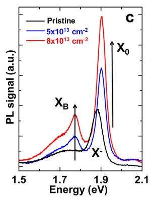
Here, the scientists found that removing chalcogen (sulfur) atoms from a 0.7-nm-thick sample of the TMD MoS2 significantly changes its optical properties. As the number of defects in the material increases, the overall brightness of the light that is emitted by the material increases. This light has a photoluminescence peak at 1.90 eV, which determines its wavelength and color. But the defects also created a new photoluminescence peak at 1.78 eV.
The scientists found that this lower energy peak dominates the photoluminescence spectrum at low temperatures, and becomes weaker as the temperature increases until it completely disappears above 250 K (-23 °C). However, at room temperature, the presence of such defects enhances the light emission. This observation goes against the conventional wisdom in the new field of 2D semiconductors, which has been that optical emission intensity at room temperature is sufficient criteria for assessing the crystal quality of 2D semiconductors; the results here suggest that assessments of crystal quality should involve low-temperature photoluminescence measurements.
The scientists also demonstrated that vacancy defects have similar effects on the optical properties of two other TMDs, MoSe2 and WSe2. These results indicate that the effects of point defects are likely universal in other 2D semiconductors, as well.
The researchers propose that the underlying mechanism of these effects depends on the interaction of the defect sites with nitrogen gas in the air. In vacuum, the defects did not have any effect on the TMDs' optical properties. The scientists explain that N2 molecules in the air may drain free electrons from the material at the defect sites, which results in a greater proportion of free excitons (electrons bound to holes) in the material. Some portion of the free excitons then get trapped and bound by the defect vacancies, forming bound excitons. Eventually, both free and bound excitons recombine radiatively and yield two distinct light emission peaks at 1.90 eV (~650 nm) and 1.78 eV (~700 nm), respectively.
Since researchers can create these defects by irradiation or thermal annealing, the defect density—and the resulting changes in the material's optical properties—can be controlled via defect engineering. This ability could lead to the production of 2D semiconductors with multiple bandgaps, multi-colored light-emission devices, and optical gas sensors, among other applications.
"With a smart design, point-defective 2D semiconductors potentially show better materials performance, which can be realized by uncovering defect physics in 2D systems," Suh said. "That's our team's ultimate goal!"
More information: Sefaattin Tongay, et al. "Defects activated photoluminescence in two-dimensional semiconductors: interplay between bound, charged, and free excitons." Scientific Reports. DOI: 10.1038/srep02657
Journal information: Nature , Scientific Reports
© 2013 Phys.org


