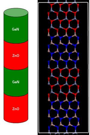
Semiconductors fabricated into stacked, nanometer-thin layers (left, schematic illustration; right, atomic structure) can harvest solar energy with striking efficiency. Credit: 2012 Elsevier
Semiconductor nanostructures are poised to play a big role in future solar-powered hydrogen generation systems, according to a new study by researchers at the A*STAR Institute of High Performance Computing. Hui Pan and Yong-Wei Zhang report that model interfaces made from gallium nitride (GaN) and zinc oxide (ZnO) semiconductors have tunable magnetic and light-harvesting capabilities—factors that can greatly improve the photocatalytic transformation of water into hydrogen fuel.
Most photoelectrochemical cells use titanium dioxide electrodes to absorb light and split water molecules into hydrogen and oxygen gas. But because this mineral has a large bandgap—a measure of energy needed to initiate photoreactions—these devices respond only to a tiny fraction of the solar spectrum. A promising way to boost this efficiency is with 'superlattice' materials that stack two different semiconductors into alternate, nanometer-thin layers. The two-dimensional channels that emerge from superlattices resemble conductive nanowires for swift charge-carrier movement. Bandgaps in these hetero-nanostructures have a demonstrated dependence on semiconductor composition and layer thickness.
Pan and Zhang investigated superlattices based on stacked GaN and ZnO layers, two semiconductors with similar electronic and structural properties that are widely used in optoelectronic devices. Using density functional theory calculations, they optimized a periodic GaN–ZnO model superlattice (see image). These computations, which describe the charge and electron spin states of materials, showed that the two semiconductor layers formed crystalline nanowire arrangements with no magnetic characteristics.
The duo then systematically introduced small defects—atomic substitutions that slightly disrupt semiconductor crystallinity—into the GaN–ZnO superlattice. To Pan and Zhang's surprise, they observed significant magnetism at several types of defect interface. According to Pan, this extraordinary activity is due to 'polar discontinuities' that form when positively charged defects partially neutralize negative charges at Ga–O interface points. Unpaired electrons then accumulate around Zn–N connections and generate magnetic forces that can boost charge separation and mobility during the reaction known as photocatalysis.
The researchers also found that engineered polar discontinuities could significantly alter semiconductor bandgaps by generating intermediate energy levels. These zones act as 'stepping stones' that make it easier for photons, or light-transmitting particles, to excite electrons for water-splitting reactions. Pan notes that once these intriguing properties of GaN–ZnO nanostructures are verified through laboratory studies, the materials may find application in energy-harvesting solar cells. "If this design proves efficient in both theory and experiment, we would then look for commercial applications by collaborating with industry," he says.
More information: Pan, H. & Zhang, Y.-W. GaN/ZnO superlattice nanowires as photocatalyst for hydrogen generation: A first-principles study on electronic and magnetic properties, Nano Energy 1, 488–493 (2012). dx.doi.org/10.1016/j.nanoen.2012.03.001


