May 2, 2013 report
New nanowire transistors may help keep Moore's Law alive

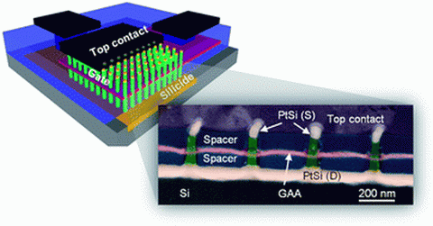
(Phys.org) —Two French researchers, Guilhem Larrieu and Xiang‑Lei Han, may have succeeded in possibly setting back the date to which Moore's Law would no longer apply by creating a new kind of nanowire Field-Effect Transistor (FET). In their paper published in the journal Nanoscale, the two describe how they built a "gate-all-around" made of 225 nanowires, each with its own 14nm-thick chromium layer that serves as a gate.
In their search to find new ways to cram more electronics onto the same size chips, researchers have turned to FETs. Transistors on chips are the parts that control the flow of electricity—figuring out a way to make them smaller is a vital part of keeping Moore's Law alive. One way to do this is to do away with wires and instead use nanowires. However, because of their small size, nanowires aren't capable of carrying enough current to do the work necessary on a chip. To get around that, researchers have tried creating bundles of nanowires; but thus far, the gates to control them have been too unwieldy. In this new effort, the researchers tried a different approach.
First they created a forest of 225 nanowires by etching a slab of silicon—the bottom half of each nanowire is submersed in a material that serves as a source. Just up from that base, the researchers applied a chromium layer wrapped all the way around the nanowire to serve as the gate. Above that was another layer of material that serves as the sink. This simple design allows each nanowire to be controlled by its individual gate, and the researchers report the thickness of the gate is what makes it all work. At 14nm, the gate can be made short enough to continue to allow for the control of the current. The result is a transistor that thus far appears to be a workable way for increasingly more circuitry to be added to a computer chip.

Should the new design pan out, it won't keep Moore's Law alive forever, of course. One day, researchers will reach a point where it's no longer possible—due to the laws of physics—to add more processing power to a computer chip. As such, new research will necessarily be focused on ways to build smarter computers using different ideas, rather than new materials.
More information: Vertical nanowire array-based field effect transistors for ultimate scaling, Nanoscale, 2013,5, 2437-2441. DOI: 10.1039/C3NR33738C
Abstract
Nanowire-based field-effect transistors are among the most promising means of overcoming the limits of today's planar silicon electronic devices, in part because of their suitability for gate-all-around architectures, which provide perfect electrostatic control and facilitate further reductions in "ultimate" transistor size while maintaining low leakage currents. However, an architecture combining a scalable and reproducible structure with good electrical performance has yet to be demonstrated. Here, we report a high performance field-effect transistor implemented on massively parallel dense vertical nanowire arrays with silicided source/drain contacts and scaled metallic gate length fabricated using a simple process. The proposed architecture offers several advantages including better immunity to short channel effects, reduction of device-to-device variability, and nanometer gate length patterning without the need for high-resolution lithography. These benefits are important in the large-scale manufacture of low-power transistors and memory devices.
via IEEE Spectrum
Journal information: Nanoscale
© 2013 Phys.org


