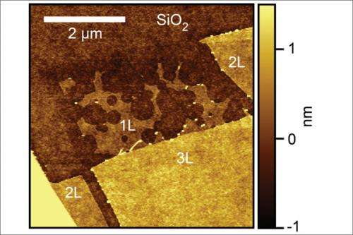
Thinnest graphene sheets react strongly with hydrogen atoms; thicker sheets are relatively unaffected

(Phys.org)—Single sheets of graphene, a curious material only 1 atom thick, are 100 times more chemically reactive than double or triple sheets, Stanford scientists say in a new paper published online Jan. 17 in ACS Nano. Understanding graphene's chemical reactivity, they say, is key to putting this unique material to work.
Graphene is a chicken-wire-like structure of carbon atoms. The highly conductive, super-light and super-strong material holds promise for applications in computing, solar energy and chemical sensing. But materials scientists are still teasing out graphene's remarkable properties and potential uses.
"The goal of the graphene community is tailoring the properties of graphene," said Stanford postdoctoral physicist Michael Neumann. "Most of these operations involve chemically modifying the material, so you need to have some idea of what the chemical reactivity of graphene is and what factors influence that reactivity."
Neumann and graduate student Georgi Diankov, both members of David Goldhaber-Gordon's physics research group, bombarded single and multiple sheets of graphene with highly reactive hydrogen atoms generated in a stream of charged gas, or plasma.
When they examined the graphene in the Stanford Nanocharacterization Laboratory, they found something surprising. The single layers of graphene were riddled with etch pits, like Swiss cheese. Thicker layers, even 1 atom thicker, were hardly pitted at all. Etch pits on the single layers outnumbered others 100 to 1.
The pits are caused by carbon atoms in graphene reacting with hydrogen atoms, presumably creating methane molecules that lift up and away out of the graphene sheet. The sheets rest on a silicon oxide "substrate," which is a participant in the etching reaction. Multilayer sheets are more protected from the substrate's effect.
The researchers also noticed that monolayer etch pits were circular, while the few etch pits found in thicker layers were hexagonal. Why the difference?
"The short answer is, we don't really know," Neumann said, but he speculates that the substrate's participation in the etch reaction could be the cause.
Graphene was famously discovered in 2004 by scientists in England who used adhesive tape to peel single layers of graphene off larger graphite flakes. Diankov and Neumann used the same technique to prepare graphene samples for their experiments.
The "exfoliated" graphene sheets can be seen with a simple optical microscope. Layered on the gray silicon substrate, the graphene looks like overlapping dark paint strokes.
Diankov is intrigued by graphene's unique properties.
"I'm fascinated by two-dimensional materials – the unusual chemistry, mechanical properties, electronic properties – and I want to explore graphene as a great model system," he said.
Stanford's facilities, like the Nanocharacterization Lab, stocked with nanoscale imaging equipment, make the university "one of the best places to do chemistry and physics on the nanoscale," Diankov said.
Next, Neumann and Diankov will test graphene reactivity with different substrates; they hope to include an experiment with no substrate at all.
Neumann admits that his work is foundational and doesn't have an immediate effect on everyday life –yet.
"Many new technologies depend on research results that are a few years, or even decades, earlier," Neumann said. "We're quite far upstream."
More information: 'Extreme Monolayer-Selectivity of Hydrogen-Plasma Reactions with Graphene,' ACS Nano (doi: 10.1021/nn304903m) dx.doi.org/10.1021/nn304903m
Journal information: ACS Nano
Provided by Stanford University


.jpg)


