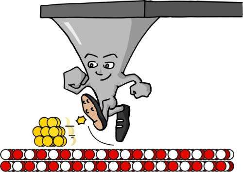
Illustration of an atomic force microscope tip “kicking” a gold cluster of atoms across a substrate. Credit: Teemu Hynninen, et al.
(Phys.org)—In nanoscience, the ultimate goal is to design better materials and devices by controlling the positions of the atoms, molecules, and molecular clusters on a substrate with exact precision. In a new study, researchers have developed a new method for controlling the movements and positions of clusters of gold atoms on an insulating substrate not only by using the tip of a microscope as is usually done, but also by using atom-sized defects in the substrate itself. The additional level of control offered by the defects could prove useful for constructing future nanodevices and nanomachines.
The researchers, Teemu Hynninen, et al., from institutes in Finland and France, have published their study on the manipulation of gold nanoclusters using defects in an NaCl surface in a recent issue of Scientific Reports.
In 1990, researchers first demonstrated that they could move single atoms by pushing them with the tip of a scanning tunneling microscope (STM). But while moving single atoms may be of great fundamental interest, it's actually more practical to be able to move somewhat larger atomic clusters.
"For many applications—such as catalysis—clusters or molecules are more relevant than single atoms, so it makes sense to operate on larger units than just atoms," Hynninen, at Aalto University and the Tampere University of Technology in Finland, told Phys.org. "Also, if you want to build something of considerable size (on the nanoscale) it's easier if you can use bigger building blocks. Of course, you would never produce anything with nanomanipulation—it's much too inefficient. Nanomanipulation is a technology with which one can design structures with absolute precision for further studies."
Over the past several years, scientists have demonstrated how to move atomic clusters using a non-contact atomic force microscope (nc-AFM), which works due to a repulsive interaction that arises between the cluster and tip when they're only a few angstroms apart. Generally, atomic clusters can be moved by a non-contact tip in two ways: by lowering the tip from directly above the cluster (which the researchers here call "kicking"), and by moving the tip toward the cluster from the side (which the researchers here call "sliding").
Although kicking and sliding provide proven ways to move atomic clusters, both methods are limited by the tip's scanning direction. That is, the direction of the cluster's movement depends on the position of the tip.
In the new study, the scientists demonstrated that, by taking advantage of the natural defects in the substrate on which the atoms lie, they can move atomic clusters in a way that is not completely constrained by the tip's position. As the researchers explain in their paper and in the YouTube video, an NaCl substrate can have vacancy defects due to missing Na ions and Cl ions. When the researchers deposited single neutral gold atoms onto the insulating NaCl substrate, they observed that the vacancies act as nucleation sites that allow the gold atoms and clusters to bond to the substrate.
Video abstract for “Defect mediated manipulation of nanoclusters on an insulator.” Credit: Teemu Hynninen, et al.
The researchers found that gold clusters bond to Na ion vacancies and Cl ion vacancies in different ways. A cluster bonds to an Na ion vacancy along one of the cluster's edges so that it orients itself with a nearby row of Cl ions. The cluster's energetically favored mode of movement is to slide along the row of Cl ions in a straight line, parallel to the bonded edge. In contrast, a cluster bonds to a Cl ion vacancy at one of the cluster's corners rather than an edge. This cluster prefers to move by pivoting around its bonded corner, as it constantly tries to reorient itself with neighboring ions. As a result, the cluster can move in a zig-zag path in any direction.
When the researchers brought in an nc-AFM to scan the surface from the top and the side, they found that they could move 5-nm clusters of gold atoms (about 2000-2500 atoms) in different ways, depending on the type of defect to which the clusters were bonded. Knowing that Na ion vacancies are the dominant defect on a part of the substrate called step-edges, and Cl ion vacancies are more common on a part called the terrace, the researchers could attribute the different types of cluster movements to the different types of vacancies. Clusters on the step-edges always moved in a straight line in a particular direction, while clusters on the terrace could be easily moved in different directions.
The defects' contributions to the movement of the clusters offer scientists an additional way to manipulate clusters using an nc-AFM. The researchers hope that this mechanism can be exploited to build nanostructures and, in a reverse process, the clusters' movements could be used to help identify the types of defects on a substrate. As the researchers explained, it may be possible to control the defects on substrates, and thereby control the movement of clusters.
"Practically all materials have defects like vacancies, and often they also appear on the surfaces," Hynninen said. "Defects can be created or removed for instance by irradiation or heat treatment. A common example is gemstone irradiation, where the color of gems is controlled by exposing them to irradiation. The radiation creates defects in the crystals and these affect the optical properties of the gems. In principle, one could use such methods to control the defects and thus movement of clusters. The exact way how this would work depends on the substrate and clusters."
More information: Teemu Hynninen, et al. "Defect mediated manipulation of nanoclusters on an insulator." Scientific Reports. DOI: 10.1038/srep01270
Journal information: Scientific Reports
© 2013 Phys.org


