September 25, 2012 feature
New LED packaging technology improves performance

(Phys.org)—Many researchers have reported improvements in LED technology by enhancing the properties of the LED itself. But the packaging that secures and protects the LED also impacts its overall performance. In a new study, researchers from Taiwan have designed a "flip glass substrate" for packaging LEDs, and demonstrated improvements in terms of a wider viewing angle, better color uniformity, and earlier identification of flaws during production compared with other LED packaging methods.
The researchers, led by Weileun Fang, a professor at National Tsing Hua University in Hsinchu, Taiwan, have published their study on the flip glass substrate LED packaging in a recent issue of the Journal of Micromechanics and Microengineering.
As the researchers explain, most commercial LEDs today are packaged in plastic leaded chip carriers (PLCCs), printed circuit boards (PCBs), ceramic holders, or similar materials. Most of these packages are partly non-transparent, so that the LED light cannot penetrate the side wall.
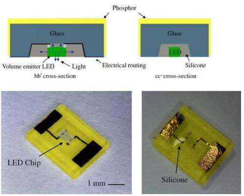
In contrast, the flip glass substrate consists of a fully transparent glass substrate covered with phosphor that has a cavity to house the LED. Silicone fills the cavity surrounding the LED for protection. When in use, the LED is flipped over so that the light emits through the back wall and side walls of the transparent glass.
"From the package structure point of view, the difference between the flip glass substrate and PLCCs or PCBs package structures are the transparent side walls and remote phosphor coating on the outside of the package rather than on the LED chip," Fang told Phys.org.
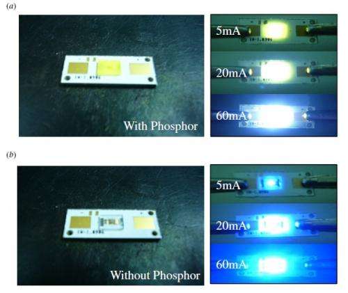
One of the biggest advantages of this new packaging system is that it provides a wide viewing angle of 140°, whereas 95% of commercial LED packages have a viewing angle of less than 125°. This improvement results from the light being able to directly penetrate the side walls of the substrate, reducing the repeated reflection loss that occurs in non-transparent packaging.

Another important LED metric is the uniformity of angular CCT (correlated color temperature), which determines the "warmth" or "coolness" of the light. Although light quality depends on several other factors, a more uniform CCT is desirable. The flip glass substrate's maximum deviation of angular CCT is 1300 K, just half of the 2500 K for other LEDs. The researchers attribute this improvement to the substrate's uniform phosphor coating on the outside of the package.
In addition, by allowing the packaging and the LED to be tested before the two components are actually put together, the fabrication process allows researchers to evaluate and fix color quality problems at an earlier stage than other types of packaging. Because this "know-good-substrate" process lets researchers know in advance that the packaged LED has good chromaticity, this advantage could cut down on fabrication costs.
"From the process point of view, the structure design allows us to sort the chromaticity coordinate before the LED chip is inside rather than after the encapsulant material is cured, as in the traditional process flow," Fang said.
Despite these advantages, the researchers note that they still have to improve the flip glass substrate's transmission, as well as perform tests on its heat dissipation and reliability. They hope that future improvements in these areas and others will make this packaging useful for high-power LEDs.
"In the process design and package structure design, we're trying to alter the current architecture of the LED package from the package end (die bond, wire bond, etc.) to the MEMS process end (wafer bonding, etc.)," Fang said. "The designed LED package should meet the specifications of applications without adopting additional optical elements (e.g., lens, collimators). In our latest study, the microstructures on the package could improve the efficiency or modify the radiation pattern of the LED package."
More information: Chien-Lin Chang-Chien, et al. "'Flip glass substrate' package technology for LED yield and performance enhancement." J. Micromech. Microeng. 22 (2012) 105039 (10pp). DOI: 10.1088/0960-1317/22/10/105039
Journal information: Journal of Micromechanics and Microengineering
Copyright 2012 Phys.org
All rights reserved. This material may not be published, broadcast, rewritten or redistributed in whole or part without the express written permission of PhysOrg.com.


