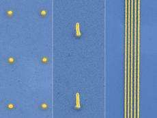
Using the new method, researchers can print dots, small towers, lines and other structures on a nanoscale. Credit: SEM images: Patrick Galliker / ETH Zurich
(Phys.org) -- Swiss researchers have developed an economic, fast and reproducible method for printing tiny structures with a simple printing method. Now they are planning a spin-off.
A line appears on the monitor and gets longer within seconds. It bends off at a right angle, changes direction several times and crosses itself on a couple of occasions until a tangle of lines emerges. Then the line grows more slowly, appears darker, stops and darkens further in a dot of a consistent size. Then it continues: a line, another dot, line, dot, line, dot.
What may sound a bit like Morse code is actually a demonstration of a new technique that ETH-Zurich researchers have developed at the Laboratory of Thermodynamics in Emerging Technologies. The method enables them to print the tiniest of structures on a micro- and nanoscale.
Using this printing method, ultrafine particles are transferred onto a surface from a capillary in a targeted fashion by way of an electrical field. Depending on how long material accumulates on the same spot, the structure grows taller, producing a nano-tower. If doctoral student Patrick Galliker, who was instrumental in developing the printer, allows them to get ever taller, they can clearly be seen toppling over on account of their proximity to the capillary. For the demonstration, Galliker uses controls similar to those found in computer games. If the researchers automatize the nano-printer using special software, it can produce the little towers autonomously, uniformly and without any connecting lines whatsoever. They can also make towers that are slightly bent or lean two of the towers against each other to form a sort of tiny arch, explains Galliker using photos he took of the structures.
The printing takes place with nano-particles of a wide variety of materials that are placed in solvents. During printing, the nano-particles accumulate next to each other according to the laws of physics. The solvent evaporates and the nano-structures, which can be smaller than 100 nanometres, are ready.
Manipulating light with nano-structures
The ETH-Zurich researchers envisage a wide range of possible applications for their new method. It is just the ticket for applications in optics, they explain. After all, light interacts differently with nano-structures than with larger objects. Surfaces that have been modified with nano-structures “manipulate the light”, as Galliker puts it. These surfaces can absorb, concentrate and conduct light instead of reflecting it. Acting as mini-antennae, the minuscule structures thus soak up the light, which falls into a kind of trap before ideally being conducted to where it is needed.
This could be used to increase the efficiency of thin-film solar cells by capturing the light and channelling it directly towards the active layer, for instance. Until now, such solar cells did not use all the light as they reflected part of it and let another part escape unused. Camouflage suits with such surfaces are conceivable, explains Dimos Poulikakos, professor of thermodynamics and head of the research group.
Moreover, using such nanostructures, new kinds of faster, more selective and highly sensitive detectors and sensors might be feasible. The nanostructures could also be used in special light microscopes in which nanoparticles increase fluorescence, Poulikakos adds, enabling the tiniest of objects, such as individual molecules, to be observed. And, of course, the nano-printer could be employed wherever material needs to be applied on a nanoscale in a targeted fashion, such as in the production of modern microprocessors: imagine, a CPU printed on the spot!
Economic and reproducible method
Using the new printing method, the tiny structures can be applied to different surfaces in a quick and reproducible manner. It is fast because the printer can be programmed in such a way that material is applied precisely where it is needed. The removal of excess material, as is necessary with other methods on a micro- and nanoscale, is no longer required, saving precious resources.
Moreover, compared to established methods that perform a similar function on a nanoscale, the new technique is considerably less expensive. It does not need enormous facilities or ultra-pure cleanrooms, exceedingly high temperatures or special pressure ratios. It thoroughly works without the otherwise necessary laborious and time-consuming vacuum steps.
As a result, the throughput and size of the printed surfaces may be increased considerably during industrial production, says Poulikakos. Additionally, prototyping at the smallest scale could perform fast and financially efficient. All this will make the method considerably more economic than the alternatives already available.
Spin-off on the cards
The researchers still have a lot of work ahead of them. For instance, they would like to develop a print head containing several individually addressable capillariesOn the one hand, such an approach will lead to an increase of throughput. On the other hand, it will enable to stack layers of different materials on top of each other opening further avenues to future products and science projects.
According to the researchers, the prospects for the new method are promising. A patent application has already been filed and the first interested parties from industry have already shown their interest. Even the foundation of a spin-off is in the pipeline. Currently, the ETH-Zurich researchers are involved in several projects with other scientists who need nano-structures that they would only be able to produce or procure themselves at great expense.
More information: Galliker P et al. Direct Printing of Nanostructures by Electrostatic Autofocusing of Ink Nanodroplets. Nature Communications, Published online, 12th June 2012. DOI: 10.1038/ncomms1891
Journal information: Nature Communications
Provided by ETH Zurich


