Sony commercializes TransferJet compatible LSI
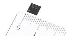
Sony today announced the commercialization of "CXD3271GW" LSI, for use in the close proximity wireless transfer technology TransferJet. This LSI realizes a 350Mbps transmission speed and the industry's highest receiving sensitivity, while also contributing to reduced power consumption, reduced parts count and smaller sizing of the sets, all to enhance its suitability for mobile devices such as smartphones. Sony recently presented this technological achievement related to its new LSI at the ISSCC (International Solid-State Circuits Conference: February 19~23, 2012, San Francisco, U.S.).
Since its commercialization of the world's first TransferJet LSI in 2009, Sony has promoted an intuitive approach to the high-speed transfer and sharing of high-resolution photos and video images whereby such high speeds are realized by simply bringing different devices, such as digital cameras and PCs, into closer proximity with each other. Meanwhile, the recent proliferation of smartphones and tablet devices has led to a consequential increase in the need for wireless communication LSIs with a lower power consumption and smaller size, together with increased demands from the mobile computing environment for further enhancements in high-speed communications and reception performance.

In order to accommodate these needs, Sony has developed the new TransferJet compatible LSI “CXD3271GW”, which achieves both a high transmission speed and the industry's highest receiving sensitivity, in addition to significantly reducing power consumption over previous models to better facilitate its implementation in mobile devices.
This LSI supports high-speed SDIO UHS-I as its host interface and introduces a new device driver design which provides a smooth and high-speed communications environment. These design enhancements have improved the new LSI's transmission speed to over 350Mbps, which is close to the theoretical maximum effective speed of 375Mbps based on the TransferJet standard. Furthermore, Sony's unique high-speed transmission technology and wideband RF-CMOS technology enables stable communications between devices, achieving the industry's highest receiving sensitivity of -82dBm (when receiving Rate65) which in fact exceeds the standard TransferJet value of -71dBm. Additionally, the RF balun, the RF switch for transmitter/receiver and the LDO and OTP-ROM, which used to be the externally embedded parts are now all pre-embedded into the new LSI, and a dedicated external crystal controlled oscillator will no longer be required by supporting a multi-reference clock. These factors contribute to a reduction in the number of parts implemented in the sets, a smaller footprint, and reductions in power consumption.
Additionally, Sony will provide a software development kit for Android to facilitate the LSI's implementation in Android devices together with the software development kit for Linux which has been provided with the previous models to developers.
Sony plans to continue to actively promote the adoption of its TransferJet LSIs by manufacturers from fast-growing markets such as smartphones.
Provided by Sony


