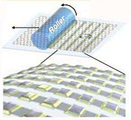
A motorized roller stripes PMMA in periodic patterns on a graphene substrate, which is later etched by a plasma treatment to make patterns in the graphene. Image credit: Kim, et al. ©2012 American Chemical Society
(PhysOrg.com) -- Finding a simple, scalable way to pattern graphene for future electronics applications is one of the biggest challenges facing graphene researchers. While lithography has been widely used to create graphene patterns for electronic devices, its multiple processing steps make it too complex for large-scale use. In a recent study, scientists have found that a motorized, movable roller can deposit a polymer solution onto a graphene surface in periodically striped and cross-striped patterns, which they used to make a transistor. By eliminating several steps involved in lithography, the new technique could lead to a low-cost method for producing graphene patterns for a variety of electronic devices on a large scale.
The researchers, from the Korea Electronics Technology Institute and Sungkyunkwan University, both in Gyeonggi-do, Korea; the Ulsan National Institute of Science and Technology in Ulsan, Korea; and Korea University in Seoul, Korea, have published their study in a recent issue of Nano Letters.
“We demonstrated how a self-assembly-mediated process can be applied to fabricate graphene micro-patterns on flexible substrates,” Professor Kwang Suh of Korea University told PhysOrg.com. “This process provides a scalable and compatible methodology for the large-scale and roll-to-roll production of graphene patterns.”
The goal of the research was to produce highly ordered patterns of PMMA polymer solution (also known as Plexiglas when in solid form) onto a single-layer graphene film prepared on a flexible substrate. The PMMA protects specific regions of the graphene while the graphene is etched by a plasma treatment. After the PMMA is washed off, graphene patterns appear etched in regions that were not covered by PMMA.
To pattern the PMMA polymer solution onto the graphene, the researchers positioned a roller on top of the graphene, and the roller was pushed by an upper motorized plate at a defined speed. When the researchers loaded the PMMA solution in a confined space formed between the roller and graphene surface, the PMMA solution edge (i.e., contact line) undergoes continuous stick-slip motion due to the competition between the pinning and capillary forces. As a result, periodically striped PMMA patterns are formed on the graphene surface over large areas.
This method produced PMMA stripes with nearly equivalent spacing and a width of about 18 micrometers. By rotating the graphene film 90°, the researchers could also fabricate cross-striped patterns.
“Our approach is not only inexpensive but also has diverse applicability, as it can run on either flexible or rigid substrates; and it is much simpler than the conventional photo-lithography process,” said Dr. Woo Seok Yan of the Korea Electronics Technology Institute.
To investigate the electronic properties of the final graphene patterns, the researchers fabricated flexible graphene-based field-effect transistors based on the patterns. After adding electrodes and an ion-gel gate dielectric, the researchers tested the transistor and found that it exhibits good electron mobility at low voltages. The same technique could be used to fabricate a variety of graphene-based devices.
“With the benefits of its simplicity, high-throughput, and scalability to the roll-to-roll processing, this process holds promise for the integration of graphene into practical electronic devices such as field-effect transistors and sensors,” Yan said.
Yan and Suh added that they plan to expand the technique to smaller scales.
“Extension of this self-assembly process may lead to an even greater variety of complex graphene patterns on the nanometer scale,” Suh said. “We are now concentrating on the high-throughput and roll-to-roll fabrication of nano-architectured graphene patterns based on this technique.”
More information: TaeYoung Kim, et al. “Large-Scale Graphene Micropatterns via Self-Assembly-Mediated Process for Flexible Device Application.” Nano Letters. DOI: 10.1021/nl203691d
Journal information: Nano Letters
Copyright 2012 PhysOrg.com.
All rights reserved. This material may not be published, broadcast, rewritten or redistributed in whole or part without the express written permission of PhysOrg.com.


