(PhysOrg.com) -- A team of researchers working out of the University of California, Berkeley, has developed an entirely new class of two-dimensional semiconductor made of indium arsenide. Called quantum membranes, the new material has a band structure and can be turned from a bulk material to a two-dimensional one, simply by reducing its size. The team, led by Ali Javey, have published the results of their findings in Nano Letters.
So-called two dimensional semiconductors can be created because of something called, quantum confinement, which is where the electronic and optical properties of a material changes as the sample size grows to a certain degree of smallness; in this case, to around 10nm or less. They, in essence, are confined to operating in a two dimensional space. Because of their unique properties, they can be put to use in highly specialized quantum optical and electrical applications. Up to now, most research on these unique semiconductors has involved using such materials as graphene. Javey and his team take another approach, creating quantum membranes (QMs) out of bands of indium arsenide
The new and unique thing about the QMs is that they can be used as a free standing material and thus can be used with a variety of substrates, unlike other such structures which are based on just a single one.
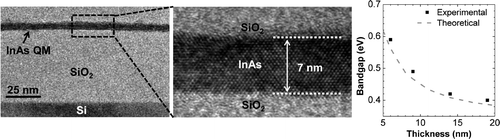
To make the QMs, the team first grows the indium arsenide in a GaSb and AlGaSb substrate. They then fashion the layer on top into whatever shape is desired; then the bottom layer is etched away. The remaining indium arsenide layer is then moved to whichever substrate is desired to make the final product.
To show the effectiveness of the resultant product, the team mapped out the optical properties of each sub-band while changing the thickness of the structure as a whole. Also, in testing the electrical properties of the new material, they found that electron mobility did not depend on the field that was applied, except in the case of very high fields, which is of course quite different from conventional semiconductors.
In addition to adding a new material to the bank available to researchers in using semiconductor materials, the results of this work also provide insight into how structurally confined materials work which could lead to more materials with truly unique properties.
More information: Quantum Confinement Effects in Nanoscale-Thickness InAs Membranes, Nano Lett., 2011, 11 (11), pp 5008–5012. DOI: 10.1021/nl2030322
Nanoscale size effects drastically alter the fundamental properties of semiconductors. Here, we investigate the dominant role of quantum confinement in the field-effect device properties of free-standing InAs nanomembranes with varied thicknesses of 5–50 nm. First, optical absorption studies are performed by transferring InAs “quantum membranes” (QMs) onto transparent substrates, from which the quantized sub-bands are directly visualized. These sub-bands determine the contact resistance of the system with the experimental values consistent with the expected number of quantum transport modes available for a given thickness. Finally, the effective electron mobility of InAs QMs is shown to exhibit anomalous field and thickness dependences that are in distinct contrast to the conventional MOSFET models, arising from the strong quantum confinement of carriers. The results provide an important advance toward establishing the fundamental device physics of two-dimensional semiconductors.
via Nanotechweb
© 2011 PhysOrg.com


