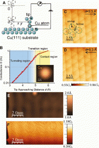
Illustration of QPCM on a Cu(111) surface. (A) Schematic model demonstrating the working principle of QPCM. The gray circles and arrows indicate the motion of the tip and the Cu atomic contact. (B) Conductance G as a function of tip approaching distance d acquired with the tip on top of a Cu adatom. (C) QPCM image with the same scan size as the inset in (B); the forward scan (from left to right) is shown. (D) Backward scan (from right to left) acquired simultaneously with the image shown in (C). (E) Constant current image of a step edge on Cu(111). Standing wave patterns originating from the surface state are clearly visible in the image. (F) QPCM image of the same area as shown in (E). The conductance decrease from top to bottom of the image is due to the plane in which the tip scans being slightly tilted with respect to the surface. Reprinted with permission from Quantum Point Contact Microscopy, Yong-hui Zhang et al., Nano Letters, July 26, 2011, Copyright © 2011 American Chemical Society
(PhysOrg.com) -- Since the first optical microscopes appeared in the late 1600s – an exact date and original inventor elude precise identification – microscopy has evolved dramatically. Scanning tunneling microscopy (STM), atomic force microscopy (AFM) and (although not generally recognized as an established method) point contact microscopy (PCM) allow scientists to view objects inaccessible to optical microscopes, with images of atoms now commonplace. Nevertheless, even this inexorable march towards ever-smaller scales has encountered limitations. (For example, STM does not provide information on local chemistry, while PCM cannot adequately image individual atoms due to it not having a single-atom contact.)
However, research conducted in the Nanoscale Science Department at the Max Plank Institute for Solid State Research in Stuttgart, Germany has demonstrated the next step: quantum point contact microscopy (QPCM), which uses single atoms at the contact between tip and surface to determine the atomic structure of conducting surfaces and, for the first time, provide images of stacked atoms in real space. Moreover, QPCM can also be used to study quantum transport, and by using molecules as the contact to potentially identify specific chemical characteristics of the scanned surface.
The research team – Yong-hui Zhang, working with Peter Wahl and Professor Klaus Kern – based their QPCM technique on low-temperature STM, and in fact QPCM operates in a low-temperature scanning tunneling microscope at ~6 K (-267 °C) in an ultra-high vacuum. However, while STM is usually operated at conductance far below a conductance quantum – a quantized unit of conductance, represented by G0 – QPCM is operated at conductances up to a few conductance quanta. “The main challenge in designing and implementing the QPCM technique,” says Zhang, “is to maintain a stable atomic configuration at the single atomic point contact during imaging, since there is large stress inside the point contact and thus the atomic configuration is often very vulnerable to any small mechanical perturbation” Since the stress in a tunneling junction is far less than in the point contact, instability at the tip apex for STM imaging is of less concern than it is for QPCM.
The team also leveraged previous research in the field. “Formation of a single atomic point contact on noble metal surfaces has been intensively studied by STM in Prof. Richard Berndt's group at the University of Kiel in Germany during the last several years,” notes Zhang. Berndt’s team showed that conductance over single silver and copper adatoms (atoms adsorbed on a surface) exhibits a smooth and reproducible transition from tunneling to contact regime, demonstrating that a stable contact can be formed as the contact tip vertically approaching a single metal adatom on noble metal surfaces. “In our work,” Zhang adds, “QPCM imaging is performed after establishing a stable contact by scanning the contact in a plane parallel to the surface in constant-height scan mode and recording the current. We found the structure of the tip apex influences strongly both the stability of the atomic contact and the image quality of QPCM, where improvements are made by training the tip apex through, for example repeated tip indentation into the metal substrate.”
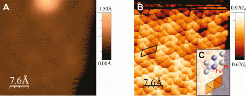
QPCM image of an iron-platinum surface alloy (FePt). (A) Tunneling constant current image of a step edge on the Pt(111) surface prepared with the FePt surface alloy before performing QPCM with the adatom (which has been put down from the tip) at the top-center of the image. Spatial inhomogeneity observed on the terrace originates from electronic states due to the alloy. (B) QPCM image of the same area as in (A); lateral displacement of less than 1 Ĺ with respect to (A) may exist. A slight increase in conductance from top to bottom is found due to piezo creep during scanning. In contrast to the tunneling image in (A), the QPCM image resolves conductance differences at the atomic scale on the alloyed terrace as well as the atomic structure of the step edge. (C) Structural model of the 2 x 1 structural unit as indicated in (B) and calculated conductance pattern associated with it. Atoms shown brighter are in lower layers (first three layers shown). The conductance pattern is obtained from a model calculation. Darker areas represent lower conductance. Reprinted with permission from Quantum Point Contact Microscopy, Yong-hui Zhang et al., Nano Letters, July 26, 2011, Copyright © 2011 American Chemical Society
Zhang also points out that the technique of QPCM imaging is itself not entirely new: Manipulated atomic imaging was first reported by J.A. Stroscio at NIST in 2004 and by Berndt’s group in 2010, where both demonstrated an adatom being laterally manipulated by the STM tip while imaging in constant-current mode. ”The manipulated atom imaging could be considered the same as the QPCM imaging,” Zhang points out, “despite the fact that they operate at different scanning mode and the former is used to operate at lower conductance. The novelty of our work lies in the QPCM study of a gold (Au(111)) surface reconstruction and an iron-platinum surface alloy (FePt), where the local atomic stacking and chemical composition are found to influence the transport current through the atomic contact.” What’s key about Zhang et al’s research is that interpreting the QPCM image is facilitated by operating in constant-height mode, and therefore feedback control of the scanning tip is not a concern.
Moreover, Zhang adds, “Our work demonstrates that QPCM can reveal more surface information than STM. Therefore the QPCM technique can be useful in the experimental research of surface characterization.”
There’s also room for improvement. “One advantage of QPCM technique is that STM and QPCM imaging can be easily combined,” notes Zhang. “In the future, it will be very nice to use a computer program to guide the scanning path of the contact during QPCM imaging, thereby avoiding areas on the surface in the STM image that can potentially destroy the atomic configuration of the contact. This measure is expected to increase the chance of success in performing QPCM imaging.”
The future also holds the possibility of QPCM have an impact on a range of devices and applications. “QPCM technique might advance the development of nanoelectronics or other relevant application,” Zhang notes. "A good understanding and control of electronic transport in nanoscale objects will help the design and development of nanoscale devices such as molecular transistors and sensors, or nanowires that interconnect nanoelectronic components. Our work demonstrates the QPCM technique can probe the influence of local atomic stacking and chemical composition on the transport conductance, thereby improve our understanding of quantum transport.”
In terms of next steps in their research, Zhang concludes, “After studying surface reconstruction and surface alloy with QPCM, the next step will be the QPCM study of electronic states on the surface. Besides the capability of probing the surface atomic stacking and chemical composition, the QPCM technique is also expected to reveal the influence of local electronic density of states on the transport current through the atomic contact.”
More information: Quantum Point Contact Microscopy, Nano Letters, doi:10.1021/nl201912u , Publication Date (Web): July 26, 2011
Copyright 2011 PhysOrg.com.
All rights reserved. This material may not be published, broadcast, rewritten or redistributed in whole or part without the express written permission of PhysOrg.com.


