(PhysOrg.com) -- On May 4, 2011, Intel Corporation announced what it called the most radical shift in semiconductor technology in 50 years. A new three-dimensional transistor design will enable the production of integrated-circuit chips that operate faster with less power. Intel’s 3-D Tri-Gate transistor will be used in 22-nanometer-technology microprocessors slated for high-volume manufacturing by the end of the year.
Intel’s breakthrough has its roots in research started in 1997 in the College of Engineering at the University of California, Berkeley. That year, a team led by professors Chenming Hu, Jeff Bokor and Tsu-Jae King Liu of the department of electrical engineering and computer sciences took up the challenge of building a transistor smaller than 25 nanometers, 10 times smaller than those in production at the time. Their work was supported by the U.S. Defense Advanced Research Projects Agency (DARPA).
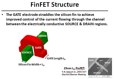
In 1999, the researchers reported a new 3-D transistor structure and gave it its widely known name FinFET. The term describes a Field Effect Transistor (FET) formed in a narrow silicon “fin” that rises above the surface of the chip. By going up, the design overcame the limitations of a flat transistor, which allows current flow to be controlled only from the top surface of the silicon channel. In contrast, current flow through a fin-shaped silicon channel can be controlled from its side surfaces, which is more effective.
Hu explains, “An analogy is to think of this channel like a vein. If you want to stop bleeding, you would pinch the vein from both sides. This would be much better than just pressing from one side.”
Further FinFET research at UC Berkeley was supported by Intel, IBM, Texas Instruments, AMD, Motorola and UMC through the Semiconductor Research Corporation, as well as DARPA.
In 2000, the Berkeley researchers predicted that FinFET technology could be scaled down to at least 10 nanometers and estimated that it would take about 10 years for the new transistor to move into high-volume production.
In its May 2011 announcement of the 3-D Tri-Gate transistor, Intel is introducing a major technical breakthrough in integrated circuit technology. The combination of performance improvement and power reduction is slated to enable innovations across a range of products, from the smallest handheld devices to powerful cloud-based computing servers.
“Scientists have long recognized the potential benefits of 3-D multi-gate transistor structures for continuing the pace of Moore’s Law,” said Mark Bohr, Intel senior research fellow. “The DARPA-sponsored Berkeley work in the 1990s, as well as earlier publications, and then Intel internal research in the 2000s contributed to developing increased confidence that multi-gate transistors would one day be the next step in transistor evolution. Academics, industry and society as a whole benefit from the mutual exchange of ideas. Both Intel and Berkeley can take pride in the fruits of university–industry partnership in research.”
Provided by University of California - Berkeley


