Panasonic today announced the development of a new technique to drastically increase the blocking voltage of Gallium Nitride (GaN) -based power switching transistor on silicon (Si) substrates. The blocking voltage of the Si substrate can be added to that of the GaN transistor by the new structure which will enable the blocking voltage over 3000V. The new GaN transistor extends the operating voltages of a variety of power switching systems including inverters for industrial use and uninterruptible power supply.
Strong electric fields are formed along to the vertical direction in the GaN transistor on a conductive Si substrate at high drain voltage. As a result, the blocking voltage is ideally determined by the sum of that by thickness of GaN and that by the Si substrate. However, experimentally observed values have been increased just by the thickness of GaN, where the blocking voltages of Si have never contributed to those.
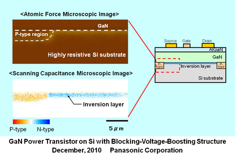
Panasonic investigates the mechanism and reveals that the increase is limited by leakage current at the interface between GaN and Si caused by electrons formed as an inversion layer.
As a technical solution for it, Panasonic proposes a new technology called Blocking-Voltage-Boosting (BVB) structure which consists of selectively formed p-type regions on the surface of the Si substrates. The p-type regions prevent the inversion electrons from flowing as leakage current.
The fabricated GaN transistor on Si with the BVB structure achieves high breakdown voltage of 2200V with the total epitaxial thickness as small as 1.9 m. This value is approximately five times higher than that in the conventional GaN transistor on Si with the same thickness of GaN. Further increase of the epitaxial thickness will enable the break down voltages over 3000V with existing epitaxial technologies. The GaN transistor on Si with the BVB structure will be applicable to various switching systems with higher operating voltages.
Applications for 99 domestic and 64 overseas patents have been filed. These research and development results have been presented at International Electron Devices Meeting 2010, held in San Francisco, U.S. from December 6 to 8, 2010.
Source: Panasonic


