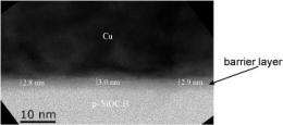
Cross-sectional transmission electron microscopy image of a barrier layer on a low-k dielectric that was formed by annealing a Cu-Mn alloy for 1 hour at 420C.
(PhysOrg.com) -- A team of international researchers is the first to uncover the chemical composition and structure of a microelectronics element that is vital to producing ever smaller - and, thus, cheaper and faster - devices.
"The number of electronic devices that can be placed within an integrated circuit has followed almost perfectly an exponential increase in the past 40 years," said James Ablett, a researcher at Synchrotron SOLEIL in France. "However, to maintain this rate, a major change in the fabrication process is required."
One of these changes involves the production of "diffusion barriers," which are needed to separate the copper metallic lines that connect the various components in an electronic device from the silicon-based insulating material. Silicon and copper are highly reactive and the mixture of the two will ultimately lead to circuit failure. However, current fabrication processes are unable to deliver diffusion barrier films that are conformal (have the same thickness across the entire interface) and thin enough - on the order of one nanometer - to support the next generation of electronic devices.
That's why Ablett, along with researchers from the NSLS, the National Institute of Standards and Technology (NIST), IMEC, and Intel, are studying one potential fabrication method that uses copper-manganese alloys. In these systems, the manganese atoms diffuse out of the alloy film upon annealing and form a thin and conformal barrier layer at the silicon interface before copper diffusion can begin.
At NSLS beamlines X27A and X23A2, the researchers used grazing incidence x-ray fluorescence spectroscopy to study these self-forming barrier layers. They grew the diffusion barrier on two different materials: thermal silicon dioxide (SiO2) and one with a lower dielectric constant.
The researchers discovered that the diffusion layer is principally made up of two different components (MnSiO3 and MnO) and is relatively easy to form on the low-k material but substantially more difficult to form on SiO2. These results are promising as low-k dielectrics, which have a low capacitance - ability to hold charge - than SiO2, will eventually be used in future microelectronic technology, enabling faster and more efficient devices. This is because insulators with a smaller dielectric constant can charge faster, allowing electrical signals to propagate faster through the circuit.
The researchers also discovered that the low-k material forms an effective diffusion barrier because its porosity helps it absorb moisture that efficiently produces the barrier's oxide layers.
Their results were published in the January 26, 2009 edition of Applied Physics Letters.
"Not only have these measurements allowed us to study the effect of the self-forming diffusion barrier process on both SiO2 and low-k dielectrics, as a function of alloy thickness, anneal temperature, and time, we also have been able to identify the major phases in the diffusion barrier layer, which will allow us to better understand how these barriers behave and to assess their ultimate feasibility for future integration into wide-scale semiconductor manufacturing," Ablett said.
More information: J.M. Ablett, J.C. Woicik, Zs. Tokei, S. List, and E. Dimasi, "Phase Identification of Self-Forming Cu-Mn Based Diffusion Barriers on p-SiOC :H and SiO2 Dielectrics Using X-Ray Absorption Fine Structure," Applied Physics Letters, 94, 042112 (2009).
Provided by National Synchrotron Light Source


