SEMATECH and NIST Collaborate on Chemical Analysis of Advanced Gate Dielectrics

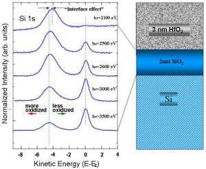
Nitrogen incorporation in thin HfO2/SiO2 film systems representative of high-k gate dielectric layers in advanced metal-oxide semiconductor field-effect transistors (MOSFETs) has been investigated by synchrotron x-ray photoelectron spectroscopy to elucidate variations in chemical composition between samples annealed in NH3 and N2 ambient as a function of temperature. In addition, depth profiling of core-level binding energy spectra has been obtained by variable kinetic energy x-ray photoelectron spectroscopy (VKE-XPS) with tunable photon energy. An HfO2/SiO2 “interface effect” has been detected in the Si 1s spectra characterized by a shift of the Si4+ feature to lower binding energy with no corresponding chemical state change observed in the Hf 4f spectra acquired over a broad range of electron take-off angles.
One of the semiconductor industry’s “grand challenges” is to develop an alternative to the SiO2 gate dielectric that has enabled scaling (increasing integrated circuit device density, according to Moore’s Law) of metal-oxide semiconductor field-effect transistors (MOSFETs) for the past 40 years. The challenge originates from the quest for integrated circuits exhibiting higher speed and lower power consumption, no longer attainable with ultra-thin (sub 2 nm) SiO2 gate dielectrics due to their high direct tunneling leakage currents. This initiative has given rise to extensive evaluation of Hf-based oxide thin films as promising high permittivity (high-k) replacement material that provides a physically thicker film with lower leakage current characteristics for equivalent SiO2 capacitance. However, intrinsic properties of hafnia, HfO2, do not satisfy all requirements for gate dielectrics, particularly, crystallization temperature, defect density, and ion diffusivity. Modification of the hafnia structure has been undertaken by various alloying efforts including nitrogen incorporation to enhance electrical performance.
Thin (3 nm) HfO2 blanket films deposited by atomic layer deposition on either SiO2- or NH3-treated Si (100) substrates have been subjected to NH3 and N2 anneal processing. High-resolution NIST measurements of synchrotron x-ray photoelectron spectroscopy (XPS) were coupled with grazing incidence x-ray diffraction (GIXRD) and electron energy loss spectroscopy (EELS) measurements to elucidate differences in chemical composition and crystalline structure resulting from anneal processing in NH3 and N2 ambient as a function of temperature to identify physical evidence for process-dependent transistor performance. Variable kinetic energy XPS (VKE-XPS), achieved via the tunable photon energy capability of synchrotron radiation, was utilized to obtain bulk thin film and interface depth profiling of the core-level electron binding energy spectra.
An “interface effect” characterized by a shift of the Si4+ feature to lower binding energy at the HfO2/SiO2 interface has been detected in the Si 1s spectra illustrated in Figure 1. However, no corresponding chemical state change was observed in the Hf 4f spin-orbit energy spectra acquired over a broad range of electron take-off angles and surface sensitivities, thereby ruling out the likelihood of Hf silicate formation at the interface. The hafnia film has been shown to getter oxygen from the underlying SiO2, thereby rendering it substoichiometric (oxygen deficient) in the neighborhood of the interface with HfO2.
The NH3 anneal ambient has been shown to produce a metastable Hf-N bond component in the Hf 4f XPS spectra corresponding to temperature-driven dissociation kinetics while the Si 2p spectra indicate Si-N bond formation near the HfO2 layer in samples exposed to 700°C/60s/NH3 anneal. GIXRD measurements identify corresponding structural changes resulting from NH2 (isoelectronic with O) exchange for oxygen in these HfO2 films, although not detected in samples exposed to anneal processing in N2 ambient. These findings are consistent with elemental profiles across the HfO2/ SiO2 /Si(100) interface determined by EELS measurements.
These SEMATECH-NIST results represent a major step toward the controlled optimization of Hf-based gate dielectrics and the development of next-generation MOSFET devices.
Source: Brookhaven National Laboratory


