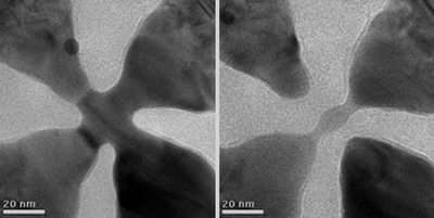
Two intersecting nanowires (left panel) were made into a four-terminal nanogap transistor (right panel) using the TEBAL method.
A research team from the University of Pennsylvania has used an electron beam to hand-carve ultra-small metal structures and devices, all with dimensions below 10 nanometers, from very thin metal sheets. Their technique could impact the development of many nanotechnologies, including nanoelectronics.
Among the structures created by the two scientists, professor Marija Drndić and graduate student Michael Fischbein, the paper's lead author, are nanodisks, nanorings, nanowires, nanoholes, and multi-terminal nano-transistors.
“Many different approaches have been undertaken to fabricate the small structures needed to probe the phenomena that take place at the nanoscale, but the most widely used and versatile techniques are limited to tens of nanometers,” Drndić said to PhysOrg.com. “Reliably and consistently fabricating devices at the sub-10-nanometer scale from the top down is generally still challenging, but our technique offers a route to this regime.”
Drndić and Fischbein used the electron beam produced inside a transmission electron microscope to essentially sculpt various metal nanostructures by removing atoms from metal films, including gold, silver, and aluminum. The films varied in thickness from 10 to 50 nanometers and were pre-cut into 80-nanometer-wide strips. This top-down approach yielded structures and devices with near atomic detail.
“It’s like using a magnifying glass and sun rays to sculpt an ice cube,” says Fischbein. “However, using an electron beam instead of sun rays allows for precision on the atomic scale.”
Among its advantages over other techniques, Drndić and Fischbein say, is the fact that theirs uses the imaging beam of a transmission electron microscope, which means the structures can be imaged with atomic resolution and inspected in real time as they are created. These characteristics result in structures with smooth surfaces (atomically speaking) and high reproducibility – creating nearly identical copies of the same structure.
Additionally, the technique (referred to as TEBAL, for transmission electron beam ablation lithography) allows the contacts between a nanostructure and its leads to be resistance-free, and thus more efficient. Structures made from bottom-up techniques, i.e., assembled from smaller components, typically first need to be placed on a chip and then connected to larger circuitry. TEBAL avoids these steps.
All of the structures created using TEBAL were done so by hand, with a human user guiding the electron beam and watching each structure take shape. “Computer control should offer an even higher degree of precision than we've demonstrated and produce highly intricate patterns over a wide area,” said Fischbein.
TEBAL has many potential applications in nanoscience because it has the ability to produce a wide variety of nanostructures. Running a current through TEBAL-created nanowires could allow them to be used as nanomagnets. Or, the wires could be used to test the effects of wire shape and size on their conductivity, using both regular and superconducting wires. The tiny transistors Drndić and Fischbein created have many uses in molecular electronics. Nanogap-nanohole devices can be used in the manufacture of single-molecule detectors and provide new opportunities for DNA nanopore sequencing.
This research is described in detail in the April 17, 2007, online edition of Nano Letters.
Citation: Michael D. Fischbein and Marija Drndić, “Sub-10 nm Device Fabrication in a Transmission Electron Microscope.” Nano Lett. ASAP Article, DOI: 10.1021/nl0703626
Copyright 2007 PhysOrg.com.
All rights reserved. This material may not be published, broadcast, rewritten or redistributed in whole or part without the express written permission of PhysOrg.com.


