They look like tiny swirling dust devils on the surface of the superconductor: "vortices" that appear where magnetic fields interact with the material. Unlike harmless dust devils, however, vortices can sap a superconductor's ability to transmit current without resistance.
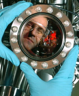
Image: Goran Karapetrov of Argonne's Materials Science Division prepares a scanning tunneling microscope. The device can determine the surface structure of a sample at the atomic scale, leading to new discoveries about the interaction of magnetic fields and high-temperature superconductors. Photo by George Joch.
View vortex video: Vortices, the small dark dots appearing in these video images (2 MB .mov file) from a scanning tunneling microscope, are where magnetic fields penetrate a superconductor and the amount of current the material can carry. From left to right, these images show the transition of "chains" of vortices. A single chain, left, splits into two chains as the magnetic field is strengthened. At right, a stronger magnetic field splits the double chain into three chains. These chains have never before been observed.
Knowing how the vortices move and arrange themselves under various temperatures and magnetic fields, as well as how they are influenced by the physical properties of the material, is critical in maintaining supercurrent flow.
As part of Argonne's intense focus on superconductors, a team of scientists in the laboratory's Materials Science Division (MSD) has obtained, for the first time, detailed images of the interaction of magnetic vortices with artificial, nanoscale engineered defects in a superconductor. Understanding this interaction could help scientists reduce the vortices' current-sapping effects — or lead to fundamentally new superconductor designs for transmitting DC and AC electric power, and quantum logic devices based on vortex manipulation.
High-temperature superconductors, discovered in 1986, have attracted intense interest due to their ability to conduct electricity without resistance when cooled with liquid nitrogen. Previously, superconductivity was only known in metals cooled with liquid helium, which is much more difficult and expensive to produce and handle. High-temperature superconductors are now used in many applications, including RF filters for mobile telephone networks, magnetic resonance imaging (MRI) machines and particle accelerators.
A critical factor limiting applications for these superconductors is their response to magnetic fields, such as in electric motors. Magnetic fields reduce the amount of current a superconducting material can carry. The fields create swirling tubes of electrical current — vortices — in the superconducting material. Superconductivity is completely suppressed within these structures. (The individual structure of vortices and their arrangement were predicted by Alexei Abrikosov of Argonne's Materials Science Division, who won the 2003 Nobel Prize in physics for his work on superconductors.) And as current flows through the superconductor, the vortices are pushed at right angles to the current flow by the Lorentz force. The vortex movement inside the material dissipates energy and produces resistance.
Scientists have discovered that vortices can be locked into position by "pinning" them to defects — tiny grains of non-superconducting substances embedded in the superconductor.
"Today, vortex pinning is the main thrust of superconductor research," said Goran Karapetrov (MSD), a lead researcher of the Argonne team that includes Maria Iavarone, Jan Fedor, Dan Rosenmann and Wai Kwok (all MSD). "We are concentrating on the microscopic physics behind defects that hold the vortices in place and increase the current-carrying capability of the materials."
To learn more about vortices and their effects, the Argonne team uses low temperature scanning tunneling microscopy, or STM. This sophisticated technique is used in fundamental research to obtain atomic-scale images of surfaces as well as essential information on the electronic states at and just beneath the surface. The atomic-scale images of the surface and its electronic structure allow the Argonne team to pin-point the positions of both the vortices that control the superconductivity and the defects that pin the vortices. Applying this powerful imaging technique to engineered defect structures is a major advance.
STM requires an extremely sharp conducting probe held close to the sample — at a distance of only a few atom-diameters. Electrons can jump the gap or “tunnel” between the sample material and the stylus, producing an electrical signal. The stylus slowly scans across the surface, raising and lowering to keep the gap between the surface and the tip constant. Recording the vertical movement of the stylus reveals the structure of the surface atom by atom.
"If the scanning tip touches the surface, the experiment is over," Karapetrov said. "These experiments are very precise. To visualize the surface, the tip comes within three to four Angstroms of the material. It has to be precisely that distance — within one hundredth of an Angstrom — in order to observe these effects."
Beyond developing sophisticated STM techniques, the team devised a method of preparing a sample with an atomically flat surface containing a periodic array of defects to pin the vortices.
"The size of each defect allows it to hold up to six vortices," Karapetrov said. "As the magnetic field increases beyond the saturation number of the defect, vortices appear outside the defect."
The vortices induced by a weak magnetic field attached themselves to the defects, as expected. As the scientists increased the magnetic field, STM images revealed additional vortices; those that couldn't find a home in a defect appeared alongside in orderly lines — a "chain." As the magnetic field was increased further, the vortex chains became denser, up to a specific, critical intensity; at this critical field the vortex chain split into two parallel chains. The transition was accompanied by a peak in the superconductor's critical current density — the measure of how well the superconductor carries large electric currents. The scientists were able to create additional parallel chains by further increasing the magnetic field.
"It's basically a phase transition," Karapetrov said. "This behavior was predicted theoretically more than 10 years ago, but it hadn't been possible to see it until this scanning technique was perfected."
The experiments marked the first time this phase transition from single to multiple chains had been directly observed. It was also the first time vortices have been studied in engineered samples with STM. Previously, creating superconductors with varying defect properties was done using randomly distributed defects created with heavy-particle accelerators like Argonne's ATLAS.
"The STM experiments using samples irradiated at ATLAS helped us a lot. But the ability to create engineered samples means we are free to make whatever geometry of defects fits best for the application," Karapetrov said. "We can design the material for vortex-pinning abilities and the best critical current by changing the fabrication parameters. Since the defects are created by lithography, we have full control over the geometry and internal structure." The lithographic process also allows researchers to vary the material in the defects, opening up a new avenue for research.
The research resulted in two published papers in Applied Physics Letters and Physics Review Letters: the first discussing the sample preparation, the second focusing on the research results. (APL 87, 162515 (2005), Phys. Rev. Lett. 95 (2005) 167002).
Source: Argonne National Laboratory


