New Self-Assembling Technique Provides Path to Manufacturing Complex Nano-Electronic Devices
In the time it takes to read this sentence, your fingernail will have grown one nanometer. That's one-billionth of a meter and it represents the scale at which electronics must be built if the march toward miniaturization is to continue. Reporting in the June 3 issue of the journal Science, an international team of researchers shows how control over materials on this tiny scale can be extended to create complex patterns important in the production of nanoelectronics.
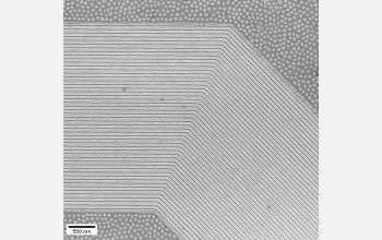
Image: The directed self-assembly process can produce large, virtually perfect arrays of bent lines at the nanoscale. Such arrays could form the basis of nanoscale electronic devices. Credit: Mark Stoykovich and Paul Nealey
About two years ago, a team led by University of Wisconsin-Madison Chemical and Biological Engineering Professor Paul Nealey demonstrated a lithographic technique for creating patterns in the chemistry of polymeric materials used as templates for nanomanufacturing. They deposited a film of block copolymers on a chemically patterned surface such that the molecules arranged themselves to replicate the underlying pattern without imperfections.
That technique works well for creating templates that are neatly ordered in periodic arrays, explains Nealey, who directs the NSF-funded Nanoscale Science and Engineering Center. "But one of the challenges of nanofabrication is integrating these self-assembling materials, that naturally form periodic structures, into existing manufacturing strategies."
Adds Nealey: "Engineers create microelectronics under free-form design principles. Not everything fits neatly into an array. This new technique directs the assembly of blends of block copolymers and homopolymers on chemically nano-patterned substrates. The result is the creation of structures with non-regular geometries. We've now potentially harnessed the fine control over structure dimensions, afforded by self-assembling materials, to allow for the production of complex nanoelectronic devices."
That kind of control is critical if computer architects are to continue advancing by Moore's Law. In 1965, Gordon Moore noted the exponential growth in the number of transistors per integrated circuit and predicted the trend would continue. It has. About every 18 months, the number of transistors in computer chips doubles. By decreasing the size of these components and, consequently, fitting more of them onto a single chip, computer speed and power improves. But before long, existing technology will run out of room.
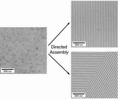
Image: Left to its own devices, the "block copolymer" mix used by the University of Wisconsin group will congeal into a disordered pattern resembling a fingerprint (left). But the directed assembly process can transform that pattern into highly ordered stripes or bends (right). These well-aligned geometries are commonly used in the nanofabrication of integrated circuits and microelectronic devices. Credit: Mark Stoykovich and Paul Nealey
Current manufacturing processes employing chemically amplified lithography techniques achieve dimensions as small as 50 to 70 nanometers, but that technology might not be extendable as feature dimensions shrink below 30 nanometers.
By merging the latest principles of lithography and self-assembly block-copolymer techniques, researchers at UW-Madison and the Paul Scherrer Institute in Switzerland developed a hybrid approach that maximizes the benefits and minimizes the limitations of each approach to nanomanufacturing.
"These new self-assembly materials used in conjunction with the most advanced exposure tools may enable the extension of current manufacturing practices to dimensions of 10 nanometers or less," says chemical and biological engineering graduate student and co-author Mark Stoykovich.
The team includes Nealey, Stoykovich, graduate student Erik Edwards, former postdoctoral researcher Sang Ouk Kim, chemical and biological engineering Professor Juan de Pablo, UW-Madison physics Associate Professor Marcus Mueller, and Harun Solak of the Paul Scherrer Institute in Switzerland.
The group conducted its work at the Center for Nanotechnology at UW-Madison's Synchrotron Radiation Center. It was funded in part by Semiconductor Research Corporation and the National Science Foundation's Nanoscale Science and Engineering Center.
Source: University of Wisconsin-Madison


