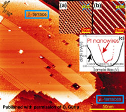
Oguzhan Gurlu and a group of scientists from University of Twente, Netherlands report about formation of Pt nanowires on Ge (001). Pt atoms adsorbed onto Ge(001) surface form extremely well-ordered nanowire arrays by self-organization after high-temperature annealing. Using scanning tunneling spectroscopy and microscopy, authors show that they are metallic and defect free. Nanowires are only 0.4 nm thick with a spacing of 1.6 nm in between, and have aspect ratios up to 1000. (Updated*)
The growing activity in the interdisciplinary area of nanometre-scale science and technology can be traced to the ever-increasing quest for the miniaturization of electronic devices, driven by the need for faster and more powerful electronics. In addition to the importance of developing new generation electronics, materials on the nanoscale often exhibit interesting quantum phenomena.
One of the examples is the electrical conductance of a metallic nanowire. Because the size of the wire is comparable to the Fermi wavelength of the conducting electrons in metal, the electrons transport ballistically along the wire and form well-defined quantum modes in the transverse direction. Such nanowires may be used as conductors and as single-atom digital switches in nanoelectronic circuits. The conductance quantization is sensitive to the adsorption of a molecule onto the nanowire which may lead to applications in chemical sensors.
Two-dimensional systems display magnetic properties distinct from bulk materials.
Co nanowires grown at Pt step edges are shown to possess unexpected magnetic properties.
However, with respect to procedures and materials used, producing nanowires is far from being trivial.
There are several problems and drawbacks that almost all techniques or produced wires suffer from.
Some require exotic elements or surfaces to form, while others do not order well or contain a lot of defects. Having unvarnished one dimensionality as well as high aspect ratio is another problem. Although metallicity is usually expected from nanowires for unusual observations, only a few may qualify to be so while missing other properties.
Authors present the formation of one-atom-thick, up to 380-nm-long, absolutely defect-free, metallic nanowires, formed by self-organization of Pt atoms on Ge(001) surface.
They studied the behavior of these nanowires, after annealing at temperatures >1000 K, using STM and STS and observed the formation of one-dimensional, defect-free, metallic nanowires with high aspect ratios.
Authors claim that Pt nanowires formation can be discussed in terms of a relativistic property possessed by heaviest 5d elements, and the pathway to their formation can be explained by dimer breakup on Ge(001) surface at elevated temperatures followed by a surface polymerization reaction.
Read the article in Applied Physics Letters (Vol 83, 22, pp. 4610-4612)
* This news review was updated after an author of the article Oguzhan Gurlu contacted PhysOrg.com and provided an STM image of Pt nanowires on Ge (001). You can use a unique opportunity to ask your questions and discuss this publication with the author. We will contact him to answer questions arisen.


