Samsung demonstrated a working carbon nanotube display prototype in 1999, and has almost completed the development of a field emission display (FED) with a 30-inch diagonal screen, according to a Korea Times report. The report said that Japan's government-backed New Energy and Industrial Technology Development Organization (NEDO) is likely to spend more than $5 million on FED projects in 2004 in an attempt to wrest leadership of display technology back from South Korea.
As the transition from Cathode-Ray Tube displays to LCD displays accelerates, various technologies are competing to replace LCDs. The current front runner for flat screens appears to be OLED displays, which have the potential to create clearer, sharper, and brighter images than LCDs. However, researchers are making steady progress with using carbon nanotubes to make displays.
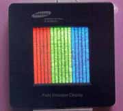
The FED is a new type of flat-panel display in which electron emitters, arranged in a grid, function individually to generate colored light. It is touted as a breakthrough technology because it can accommodate a thin panel like liquid crystal display (LCD) and offers a wider field-of-view and higher image quality. Field-emission displays use much less power than plasma displays because they’re intrinsically more efficient.
The nanotube-based cathodes in this case are created using a process proprietary to Samsung in which a combination of multi and single-wall tubes are mixed into a photosensitive resin. The resin is then screen-printed onto the cathode backplane and photoexposed to define the cathode regions. Samsung’s device differs from most field-emission displays using so-called lateral field emitters.
Full story: Korea Times


