Breakthrough in Nanoscale Understanding of Metal Shape Change

A nanocrystalline metal is one whose average grain size is measured in billionths of a meter, much smaller than in most ordinary metals. As the grain size of a metal shrinks, it can become many times stronger, but it also usually loses ductility. To take advantage of increasing strength with decreasing grain size, researchers must first understand a fundamental problem: by what processes do nanosized crystals of metal stretch, bend, or otherwise deform under strain?
A team of researchers headed by Scott X. Mao of the Mechanical Engineering Department of the University of Pittsburgh, working at the National Center for Electron Microscopy (NCEM) at the Department of Energy's Lawrence Berkeley National Laboratory, and using high-quality samples of nickel prepared at DOE's Sandia National Laboratories, has now identified a prominent way in which nanocrystalline metals deform. The researchers report their findings in the July 30, 2004 issue of Science.
Ordinary coarse-grained metals deform when parts of a grain slip past one another as extra planes of atoms, called dislocations, move through the material. The process has been compared to moving a rug by flapping one end of it to create a wave, causing the rug to inch along bit by bit. But the trick won't work if the rug is too short; likewise, if the dimensions of the crystal grains are too small, dislocations can't be created or glide through the grain to allow deformation.
Theorists have proposed that when grain sizes are too small for dislocations, a different mode of deformation comes into play: the grain boundaries themselves move, sliding past one another and allowing the grains to rotate to find new ways of fitting together.
"It's a simple idea," says Zhiwei Shan of Mao's laboratory at Pitt, "and many groups have researched aspects of it, but no one has reported direct evidence of a shift from dislocation-mediated deformation to grain-boundary-mediated deformation." Indeed, no one was sure where to look for the transition from one mode of deformation to the other. When the grains were reduced to 20 nanometers across? Ten? Perhaps as small as five?
To search for the effect, Shan used NCEM's In-Situ Microscope, which he calls "the best in America" for this kind of research. NCEM's Eric Stach explains that what makes the In-Situ's otherwise standard transmission electron microscope unique is that it combines a stage area in which samples can be stressed or manipulated in other ways — and meanwhile videotaped — with a high voltage, 300-kilovolt electron beam that can penetrate thick samples and yield excellent 1.9-angstrom resolution.
The nanocrystalline nickel samples were mounted in a probe that placed them under load — stretched them, in fact — while images of small regions of the sample were captured on videotape at the standard rate of 30 frames per second.
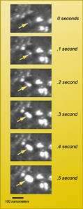
But besides having an excellent instrument, says Stach, Zhiwei Shan made a crucial observation. An effect that was far from obvious in the most common TEM imaging method, called bright-field imaging, stood out clearly with the different technique of dark-field imaging.
"As the TEM's electron beam passes through a sample, some of the electrons are diffracted," Stach explains. "Bright-field images are constructed using the direct electrons, while dark-field images use the diffracted electrons. In bright-field imaging, regions of the sample that scatter a lot of electrons, like defects such as dislocations, look darker. With dark-field images, strongly diffracting regions look brighter."
Shan agrees that "dark-field imaging was critical to the result." For when he viewed videotapes of the nickel sample under strain, he saw small regions rapidly brightening and growing larger — direct confirmation of grains sliding and rotating into positions of strong diffraction.
In a bright-field image these grain-boundary processes would have been impossible to distinguish from lattice dislocations, which in prior attempts is what other groups assumed they were seeing. It took dark-field observations to confirm that below a certain size, grain-boundary rotation indeed becomes prominent. The cut-off isn't sharp, however.
"It's continuous, not a sharp change," says Shan. "In describing grain-boundary deformations we chose the word 'prominent' carefully, because even in nanocrystalline metal, dislocations still play a role." Trapped dislocations in the crystal lattice were observed even when the average grain size was as small as 10 nanometers.
Says Stach, "The material always chooses the easiest pathway to deform, and that can differ through a range of sizes." Although the In-Situ Microscope observations confirm the grain-boundary model of nanocrystalline deformation, whichever process predominates at a given grain size depends on a variety of conditions.
"Grain boundary-mediated plasticity in nanocrystalline nickel," by Zhiwei Shan, Eric A. Stach, Jörg M. K. Wiezorek, James A. Knapp, David M. Follstaedt, and Scott X. Mao, appears in the July 30, 2004 issue of Science.
The Berkeley Lab is a U.S. Department of Energy national laboratory located in Berkeley, California. It conducts unclassified scientific research and is managed by the University of California.
Source: Berkeley Lab


