High Resolution Printed Circuit Boards with Conductors Down to 10 µm Wide

With ever increasing demands for greater miniaturisation and the use of flexible circuitry the need for improved fabrication methods for high resolution printed circuit boards is becoming more important. By precise control of the etching process inventors from the University of Oxford have been able to make the reliable production of High Resolution Printed Circuit Boards (PCBs) with conductors down to 10 µm wide more of a cost effective reality.
PCBs currently include conductors as narrow as 150 µm, but there is now a requirement for conductors to be as narrow as 25 µm and even down to 10 µm. With current manufacturing techniques it is not possible to attain the required precision especially where the spacing between the conductors varies. The etching rate is highest where the conductors are furthest apart. This leads to over-etching and subsequent under-cutting of the very fine conductors in these areas. The resultant PCB has copper conductors of variable width, and its performance is, therefore, not optimum.
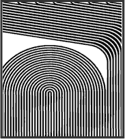
By controlling the etch conditions and the area to be etched the Oxford inventors have reduced the amount of over-etching to an acceptable level and under-cutting has been virtually eliminated. The spaces between the conductors are now all of uniform width, but with more redundant copper remaining on the PCB; the etching has been confined to narrow tracks. In the magnified view of an actual PCB the white areas represent the exposed copper tracks, while the black show the intervening non-conducting substrate.
This technology will benefit many of the applications that now demand PCBs with fine conductors or alternatively require flexible circuitry to facilitate yet further miniaturisation. Typically these include applications such as mobile phones, personal flip-top organisers and inkjet printers.
This invention is now the subject of a patent application and companies interested in developing this technology commercially are invited to contact Isis Innovation.
More information: www.isis-innovation.com/


