'Millipede' small scale MEMS prototype shown at CeBIT
Nanomechanical data storage device from the IBM Zurich Research Laboratory, Switzerland
Given the rapidly increasing data volumes that are downloaded onto mobile devices such as cell phones and PDAs, there is a growing demand for suitable storage media with more and more capacity. At CeBIT, IBM for the first time shows the prototype of the MEMS*- assembly of a nanomechanical storage system known internally as the "millipede" project. Using revolutionary nanotechnology, scientists at the IBM Zurich Research Laboratory, Switzerland, have made it to the millionths of a millimeter range, achieving data storage densities of more than one terabit (1000 gigabit) per square inch, equivalent to storing the content of 25 DVDs on an area the size of a postage stamp.
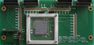
Image: "Millipede" small scale MEMS prototype compatible with SD form-factor: MEMS assembly (16.5 mm × 17.5 mm × 1.2 mm) encompassing the 2D cantilever read- and write-array, the micro-scanner, and the polymer medium.
Thousands of extremely fine tips "write" tiny pits representing individual bits into a thin film of highly specific polymer. The principle is comparable with the old punch cards, but now with structural dimensions in the nanometer scale and the ability to erase data and rewrite the medium.
The high storage density of more than a terabit was achieved by using individual silicon tips to create pits approximately 10 nanometers in diameter, i.e. 50,000 times smaller than the period at the end of this sentence. Experimental chips have been designed comprising more than 4,000 of these tips arrayed in a small 6.4 mm x 6.4 mm². These dimensions make it possible to pack an entire high-capacity storage system into the SD flash memory format package.
Technical product feasibility in terms of storage density, performance and reliability was demonstrated in recent experiments using the prototype on display. While current storage technologies are gradually approaching fundamental limits, the nanomechanical approach has enormous development potential: storage densities which correspond to the size of molecular structures may even be possible. Moreover, the nanomechanical data medium has been optimized to use a minimum amount of energy. Thus, it is ideally suited for use in mobile devices such as digital cameras, cell phones and USB sticks. Other possible applications include lithography on the nanometer scale, as well as atomic and molecular manipulation.
At CeBIT, a video microscope provides a look inside the storage unit that reveals, for example, how the polymer surface is moved across the tips with the help of a micromechanism (MEMS). An animated illustration shows how the parallel tips of the read and write array operate and how the individual tips work, and thus explains what is happening on the nanometer scale.
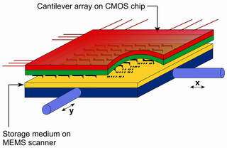
Image: The "millipede" concept: For operation of the device, the cantilever tips are brought into contact with the storage medium — a thin film of a specific cross-linked polymer coated on a silicon substrate, which is moved in the x- and y-directions for reading, writing, and erasing. The storage medium is positioned with nanometer-scale accuracy relative to the cantilever array. The tips can independently read, write or erase the bits.
Technological background
At the heart of the "millipede" technology is a two-dimensional array of V-shaped silicon cantilevers, each 70 micrometers (thousandths of a millimeter) long. At the end of each cantilever there is apart from the tip a micrometer-sized sensor for reading as well as a heating resistor above the tip, which is needed for writing. The cone shaped tip is just under one micrometer in length and has a radius of a few nanometers at its apex. The cantilever cells are arranged in the form of an array on a 10 mm x 10 mm chip. One of the recent array designs comprises a total of 4,096 (64 x 64) cantilevers. The MEMS elements are etched out of a silicon single crystal using existing technologies. The actual data medium is a thin polymer film coated on a silicon substrate. The tips can independently read, write or erase the bits.
A sophisticated design ensures that the tips are held level above the storage medium with high precision and that external vibrations and impacts are absorbed. To increase the data rate, read- and write-electronics are used that allow the operation of multiple tips in parallel. Electromagnetic actuation moves the storage medium very precisely in the x and the y-direction so that each tip can read and write within its storage field of 100 micrometers on a side. These short distances are crucial for achieving fast access times.
For the device to perform its reading, writing, erasing or overwriting functions, the tips are brought into contact with the polymer. Bits are written by heating the tip to a temperature above the glass transition temperature of the polymer by means of the heating resistor integrated in the cantilever. The polymer in close proximity to the tip is heated and becomes softer allowing the tip to indent a few nanometers into the film mechanically stressing the material. For reading, the cantilever's reading sensor, which is separate from the tip, is heated slightly. As the polymer film is scanned under the tip, the tip moves in and out of the written indentations. When the tip moves into an indent, it cools down because of the reduced distance to the substrate. This cooling results in a measurable change in electrical conductivity of the sensor. To overwrite data thermo-mechanical effects are used. They cause the stressed polymer material closely around a newly created bit to relax. Thus, existing pits can be erased by creating very close new ones. More than 10,000 writing and overwriting cycles have proved the concept's suitability as a reusable storage medium.
* Micro-electro mechanical system.


