New etching process builds custom nanostructures for X-ray optics

Scientists at the Department of Energy's SLAC National Accelerator Laboratory have invented a customizable chemical etching process that can be used to manufacture high-performance focusing devices for the brightest X-ray sources on the planet, as well as to make other nanoscale structures such as biosensors and battery electrodes.
"The tools researchers use to manipulate X-rays today are very limited," said Anne Sakdinawat, an associate staff scientist at SLAC's Stanford Synchrotron Radiation Lightsource (SSRL) who developed the new "V-MACE" process with Chieh Chang, an SSRL research associate.
"Our new technique for fabricating high performance X-ray optics involves just a few chemicals in a simple, easy-to-implement, one-step technology," Sakdinawat said. "It offers significant advantages in many far-ranging applications." The patent-pending technique is detailed in the June 27 edition of Nature Communications.
Focusing X-rays, particularly higher-energy or "hard" X-rays, is particularly challenging at the nanoscale, though it is key to the success of many scientific studies at two of SLAC's DOE Office of Science user facilities, SSRL and the Linac Coherent Light Source (LCLS) X-ray laser.
It is also of great interest for commercial applications such as X-ray microscopy, complex electronics, and biomedical devices and imaging tools.

Existing tools for focusing hard X-rays, such as specialized mirrors and sequences of concave metal structures that form lenses, are generally limited in how they can shape the X-ray light. Focusing the highest-energy X-rays to produce crisp images remains a challenge, as the focusing tools themselves generally lack nanoscale precision and sap away much of the X-ray energy.
"It's been technologically very difficult to fabricate structures that offer both high resolution and high efficiency," Sakdinawat said, and the effectiveness of the structures, which are examples of X-ray "diffractive optics," is typically based on the height and precision of their features.
The new fabrication technique is adapted from a process used to create hairlike silicon wires for research on advanced batteries and electronics. It can fabricate structures up to 100 times as tall as they are wide, with dimensions accurate to billionths of a meter. The technique reduces the need to stack multiple layers to create tall structures.
The researchers used the etching technique to build tall, precise X-ray diffractive optics, called zone plates, whose thinly spaced lines, symmetric rings or spiral patterns alternately obstruct or phase-shift X-rays and allow them to pass through in a way that separates and refocuses them. This improves the focus and produces higher-quality images.
"Basically, this is like an artificial crystal," Sakdinawat said, diffracting the X-ray light in a predictable pattern, as a crystal would. "You can basically manipulate the light in whatever fashion you want – you can shape the light in different ways," she said, based on the design of the optics and the needs of the experiment.
 image of a zone plate pattern produced using a chemical etching technique invented at SLAC. Credit: Chieh Chang, Anne Sakdinawat")
Sakdinawat and Chang tested and imaged a sample zone plate at SSRL, and they hope to construct similar plates for use in experiments at SSRL and LCLS.
The same technique can be used to build other types of precise silicon and metal-coated nanostructures, such as filtration devices, thermoelectric devices that can create electricity from heat and components for tiny bio-sensors that can be embedded in the body, and researchers are working to tailor the process to suit the needs of government agencies and corporate partners.
-
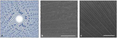
Figure a shows a computerized image of metal interconnections and zone plate buttresses in a spiral zone plate design. Figures b and c show scanning electron microscope images of metallized patterns produced by a chemical etching technique developed at SLAC. The white scale bars are 5 microns in length. Credit: Chieh Chang, Anne Sakdinawat -
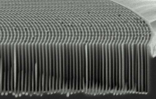
This scanning electron microscope image shows a cross-sectional view of a zone plate produced using a patent-pending chemical etching technique called "V-MACE" developed at SLAC. Credit: Chieh Chang, Anne Sakdinawat
"We're trying to expand into other fields," Sakdinawat said. "There are many different applications for this."
More information: "Ultra-high aspect ratio high-resolution nanofabrication for hard X-ray diffractive optics." Chieh Chang and Anne Sakdinawat, Nature Communications, 27 June 2014 DOI: 10.1038/ncomms5243
Journal information: Nature Communications
Provided by SLAC National Accelerator Laboratory


