Philips develops ingenious 3D interconnections for System in Package technology - Smart thinking gives you smart connect
There is a continuous drive towards further integration and miniaturization in electronic modules and components. This generates a constant need for new or improved manufacturing technologies for IC's and IC based modules. Philips CFT (Centre for Industrial Technology) has developed an ingenious 3-dimensional interconnection pattern technology based on photolithography using inclined UV exposure, resulting in relatively lower costs, miniaturization and more design freedom.
The world of consumer electronics today focuses on miniaturization: smaller cell phones, smaller electronics, and on top of that more and more additional functions. Manufacturers, on the other hand, are challenged to safeguard cost efficiency, reliability in these increasing smaller physical dimensions. This means new ways and technologies for cost-efficient manufacturing to achieve this miniaturization must be developed. Philips is in the forefront of these new developments. System in Package and interconnect technologies provide solutions.
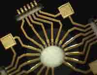
To keep electronics devices, like cell phones, small, Philips CFT has developed smart 3-D interconnection patterns on multi-chip modules. The patterns are made with a 3-D lithographic method where phase gratings are incorporated in the photo mask. The phase gratings cause local inclination of the UV beam, which is then used to expose the side walls, so making the connections from the top to the bottom of a substrate. This technology offers manufacturers more freedom; patterns on the side walls of any shape become possible.
By applying these design principles many components or modules can be developed with improvement in performance and functionality. Typical examples are miniature power transformers, antennas, high Q inductors, and micro-optical-electrical-mechanical systems (MEMS and MEOMS). This method is also of great importance for chip scale and wafer scale packaging, and for multi-chip modules.
Source: www.philips.com


