Silicon oxide circuits break barrier: Nanocrystal conductors could lead to massive, robust 3-D storage

Rice University scientists have created the first two-terminal memory chips that use only silicon, one of the most common substances on the planet, in a way that should be easily adaptable to nanoelectronic manufacturing techniques and promises to extend the limits of miniaturization subject to Moore's Law.
Last year, researchers in the lab of Rice Professor James Tour showed how electrical current could repeatedly break and reconnect 10-nanometer strips of graphite, a form of carbon, to create a robust, reliable memory "bit." At the time, they didn't fully understand why it worked so well.
Now, they do. A new collaboration by the Rice labs of professors Tour, Douglas Natelson and Lin Zhong proved the circuit doesn't need the carbon at all.
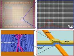
Jun Yao, a graduate student in Tour's lab and primary author of the paper to appear in the online edition of Nano Letters, confirmed his breakthrough idea when he sandwiched a layer of silicon oxide, an insulator, between semiconducting sheets of polycrystalline silicon that served as the top and bottom electrodes.
Applying a charge to the electrodes created a conductive pathway by stripping oxygen atoms from the silicon oxide and forming a chain of nano-sized silicon crystals. Once formed, the chain can be repeatedly broken and reconnected by applying a pulse of varying voltage.
The nanocrystal wires are as small as 5 nanometers wide, far smaller than circuitry in even the most advanced computers and electronic devices.
"The beauty of it is its simplicity," said Tour, Rice's T.T. and W.F. Chao Chair in Chemistry as well as a professor of mechanical engineering and materials science and of computer science. That, he said, will be key to the technology's scalability. Silicon oxide switches or memory locations require only two terminals, not three (as in flash memory), because the physical process doesn't require the device to hold a charge.
It also means layers of silicon-oxide memory can be stacked in tiny but capacious three-dimensional arrays. "I've been told by industry that if you're not in the 3-D memory business in four years, you're not going to be in the memory business. This is perfectly suited for that," Tour said.
Silicon-oxide memories are compatible with conventional transistor manufacturing technology, said Tour, who recently attended a workshop by the National Science Foundation and IBM on breaking the barriers to Moore's Law, which states the number of devices on a circuit doubles every 18 to 24 months.
"Manufacturers feel they can get pathways down to 10 nanometers. Flash memory is going to hit a brick wall at about 20 nanometers. But how do we get beyond that? Well, our technique is perfectly suited for sub-10-nanometer circuits," he said.
Austin tech design company PrivaTran is already bench testing a silicon-oxide chip with 1,000 memory elements built in collaboration with the Tour lab. "We're real excited about where the data is going here," said PrivaTran CEO Glenn Mortland, who is using the technology in several projects supported by the Army Research Office, National Science Foundation, Air Force Office of Scientific Research, and the Navy Space and Naval Warfare Systems Command Small Business Innovation Research (SBIR) and Small Business Technology Transfer programs.
"Our original customer funding was geared toward more high-density memories," Mortland said. "That's where most of the paying customers see this going. I think, along the way, there will be side applications in various nonvolatile configurations."
Yao had a hard time convincing his colleagues that silicon oxide alone could make a circuit. "Other group members didn't believe him," said Tour, who added that nobody recognized silicon oxide's potential, even though it's "the most-studied material in human history."
"Most people, when they saw this effect, would say, 'Oh, we had silicon-oxide breakdown,' and they throw it out," he said. "It was just sitting there waiting to be exploited."
In other words, what used to be a bug turned out to be a feature.
Yao went to the mat for his idea. He first substituted a variety of materials for graphite and found none of them changed the circuit's performance. Then he dropped the carbon and metal entirely and sandwiched silicon oxide between silicon terminals. It worked.
"It was a really difficult time for me, because people didn't believe it," Yao said. Finally, as a proof of concept, he cut a carbon nanotube to localize the switching site, sliced out a very thin piece of silicon oxide by focused ion beam and identified a nanoscale silicon pathway under a transmission electron microscope.
"This is research," Yao said. "If you do something and everyone nods their heads, then it's probably not that big. But if you do something and everyone shakes their heads, then you prove it, it could be big.
"It doesn't matter how many people don't believe it. What matters is whether it's true or not."
Silicon-oxide circuits carry all the benefits of the previously reported graphite device. They feature high on-off ratios, excellent endurance and fast switching (below 100 nanoseconds).
They will also be resistant to radiation, which should make them suitable for military and NASA applications. "It's clear there are lots of radiation-hardened uses for this technology," Mortland said.
Silicon oxide also works in reprogrammable gate arrays being built by NuPGA, a company formed last year through collaborative patents with Rice University. NuPGA's devices will assist in the design of computer circuitry based on vertical arrays of silicon oxide embedded in "vias," the holes in integrated circuits that connect layers of circuitry. Such rewritable gate arrays could drastically cut the cost of designing complex electronic devices.
More information: pubs.acs.org/doi/abs/10.1021/nl102255r
Provided by Rice University


