Toshiba develops essential technology for spintronics-based MOS field-effect transistor
(PhysOrg.com) -- Toshiba Corporation today announced that it has developed MOSFET cell based on spin transport electronics, or spintronics, an advanced semiconductor technology that makes use of the spin and magnetic moment inherent in electrons. Toshiba has fabricated a spintronics cell and verified its stable performance for the first time, and will present full details of the cell and its technologies on December 7 (EST), at the International Electronics Devices Meeting in Baltimore, Maryland, U.S.A.
Continuing advances in MOSFET devices based on current miniaturization technologies will inevitably hit a wall as they meet such problems as relative degraded performance due to the increase in the resistance of global wiring and increased power consumption due to current leakage. Spintronics is regarded as a major candidate among potential solutions to this problem, but its application in a transistor has only recently started and has only been partially proved.
Electrons in a magnetic layer naturally are spin polarized in one of two spin states, spin up or spin down, and the majority state determines the spin state. These spin states are more or less permanent in a magnetic layer, realizing a nonvolatile characteristic that can be used to store data. Spin current can be flowed into the same spin state in a magnetic layer, and this capability changes the impedance characteristics, which determine the read signal of a spin device.
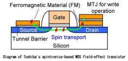
Toshiba has introduced magnetic layers into the source and drain of a MOSFET cell, and successfully applied these to controlling spin direction by the spin-transfer-torque-switching (STS) method, and by applying gate and source/drain voltages. A magnetic tunnel junction is applied for write operation of STS in the magnetic layers, which are formed with full-Heusler alloy, an intermetallic that acts as a high spin polarizer.
Toshiba confirmed the practical performance in transistor level of the scalable spintronics-based MOSFET device that promises fast random write and access speeds with low power consumption. It opens the way to next-generation non-volatile semiconductor devices that can be used as reconfigurable logic devices, and non-volatile LSI chip with memory function. Toshiba will promote development toward establishing fundamental technologies for application after 2015. This work was partly supported by the New Energy and Industrial Technology Development Organization (NEDO) in Japan.
Source: Toshiba Corporation


