The perfect cut

You need the right tool to slice silicon blocks into paper-thin wafers: a several-kilometer-long wire wetted with a type of grinding paste. And all the parameters must be optimally adjusted -- only then can significant material losses be avoided during the cutting process.
The ability to cut onions into thin slices isn't just a matter of practice - choosing the right implement also helps make good onion rings. The same principle applies when cutting silicon blocks to make wafers for solar cells.
You need a special slicing tool to produce paper-thin wafers from silicon blocks ("ingots"): reminiscent of an egg slicer, a filigree wire is used to cut through the ingot at a speed of up to 60 km/h. This wire is several hundred kilometers long and arranged in such a way that the ingot is sliced into hundreds of wafers simultaneously. The process takes around six hours and the resultant slices are approximately 180 µm thick.
Dr. Rainer Kübler, business unit manager at the Fraunhofer Institute for Mechanics of Materials IWM, explains: "When slicing the wafers, the challenge is to reduce the saw gap width." The space between two wafers is governed by the thickness of the wire. The steel wire is wetted with a type of paste ("slurry"), a mixture of silicon carbide and polyethylene glycol. This is harder than silicon and cuts through the ingot. The gap arises where the silicon is reduced to powder during cutting. "Gap widths are currently around 180 µm," says Kübler, "which means that given a wafer thickness of 180 µm, we generate the same amount of waste for each silicon slice. That's inefficient." The researchers "want to achieve smaller saw gap widths of around 100 µm, which are also suitable for industrial applications."
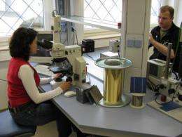
In a project funded by the federal ministry for the environment (BMU), they are currently studying the abrasion process and contact regimes using a single-wire saw and are principally interested in the interactions between the wire, the slurry and the silicon. They are also using computer modeling to simulate different configurations. What forces are at work when sawing with thin wires? How can one ensure the wire is well wetted? What is the best grain size for the slurry and how must the particles be distributed?
"We want to answer all these questions and ultimately arrive at optimal wire and slurry systems that are suitable for industrial applications," says Kübler. The researchers are currently striving to achieve gap widths of 90 µm, which would represent a huge increase in efficiency as waste would be halved.
Source: Fraunhofer-Gesellschaft (news : web)


