Scientists Shed 'Light' on Semiconductor Quandry

(PhysOrg.com) -- UC San Diego scientists are using laser plasma-produced light sources to explore performance improvements of critical inspection tools for the semiconductor industry, which ultimately will enable industry to pursue even better and faster chips. While optical lithography is being pushed to its limits in the semiconductor industry, there is a growing concern whether metrology tools can keep pace for creating and inspecting the new generation of devices.
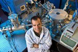
In his lab at the UCSD Jacobs School of Engineering, Mark Tillack - a research scientist in the Department of Mechanical and Aerospace Engineering and Associate Director of the Center for Energy Research - is working on this very problem via a two-year UC Discovery Grant from semiconductor equipment manufacturer KLA-Tencor.
A year ago, the semiconductor industry was concerned whether or not a sufficiently high powered light source could be developed for high volume manufacturing. Recent progress in that area has instilled confidence that a transition to EUV (Extreme Ultraviolet) wavelengths is feasible. Now, the industry has begun to shift its focus to what is called “actinic metrology” light sources, Tillack said. Attaining acceptable yields in the manufacturing of advanced photo masks, for example, will require higher performance optical metrology tools. The key to improving these tools is the development of new extreme ultraviolet light sources that operate at the actinic wafer exposure wavelength. Metrology essentially uses the same wavelength to measure the structure as was used to create it. Photo mask inspection is a form of actinic metrology. (Actinism is a property of radiation that leads to the production of photochemical effects).
“Our research group is branching out into the latest topic of active interest in the semiconductor manufacturing industry, which is EUV actinic metrology applications,” Tillack said. “This grant from KLA-Tencor will enable us to apply our scientific expertise to this new and challenging problem that is critical for EUVL (Extreme Ultraviolet Lithography) to flourish. …We’re basically trying to make the light source small enough and stable enough to provide them with the high resolution they need. They are taking our light source, manipulating it onto optics and bringing it onto a mask or wafer, trying to achieve resolution down to tens of nanometers.”
Today, the smallest features on a microchip in volume production are created using 193-nanometer excimer laser sources focused through the scanner optical path that includes water between the lens and the wafer to generate critical dimensions 45 nanometers or smaller. Within the next decade, next-generation extreme ultraviolet light sources will produce light with a wavelength of 13.5 nanometers.
“In photolithography, the mask contains the pattern to be transferred to the substrate, which eventually becomes the semiconductor device after numerous other treatments,” Tillack explained. “Light - in our case from the laser plasma - passes through, or reflects off of the mask and then onto the substrate. So, the substrate is exposed to the pattern on the mask. It’s similar to photography, where the ‘mask’ would be the negative. The idea is that all the devices that will use EUV light must be very accurate in that part of the spectrum. One example is the mask. If the mask is not created very accurately, then the exposure of chips will be bad. Masks can be very expensive, and manufacturers go through a lot of trouble to inspect their masks before putting them into production.

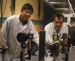
“There are some aspects of laser plasma we have found might help solve the industry’s problem,” Tillack added. “The metrology problem is different than the manufacturing problem in that the requirements on the light sources are different. For manufacturing, you need lots of power (EUV); for metrology you don’t need a super powerful source, but it has to be a highly controlled source. We’re trying to figure out whether we can create and maintain a very small plasma emitting the light and have it reproducible over time. …What we’re learning here may open an avenue for a metrology light source for EUV lithography.”
To maintain quality of the patterns on photo masks used in lithography, KLA-Tencor builds pattern inspection systems. Dan Wack, senior director of advanced technology at KLA-Tencor, said scaling the critical dimensions in the lithography process will help reduce chip costs.
“The results of this research (that Mark Tillack is doing) will enable industry to build cost-effective light sources for inspection systems,” Wack said.
Wack said collaborating with researchers like Mark Tillack provides KLA-Tencor with a deeper understanding of the fundamental issues on this emerging technology.
“Some of our latest products will take us forward three to five years but this research will enable product development in four-to-six years for our process control systems,” Wack said. “Mark’s team has advanced tools and the skilled researchers who can understand the behavior of these laser-produced plasmas in this new size regime. I think this research will have a big impact.”
Tillack said this research will also help the American semiconductor industry maintain its competitiveness.
“The United States was a leader in the development of semiconductor lithography, but the old tools went overseas,” he said. “I think the semiconductor industry, especially in California, is well aware that you cannot dominate and stay ahead of the world in any high tech area unless you keep moving forward. EUV Lithography might save the semiconductor industry in this country. It will give us another 10-to-20 years of leadership. We will lose market share if we don’t stay ahead of the competition.”
Provided by University of California - San Diego (news : web)


