Industry's first mass production of DRAM in 90nm technology
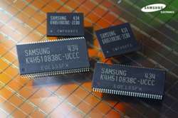
Samsung Electronics Co., Ltd., the world leader in advanced semiconductor memory technology, announced today the industry's first mass production of 90nanometer (nm) 512Mb DDR SDRAM on 300mm base wafers. Samsung pioneered nanometer level production technology in 2003 with production of 2Gb NAND flash memory in a 90nm process.
The 90nm 512Mb DDR SDRAM with voltage rates of 2.5V is available at both 400 and 333MHz. The new device is already being verified by leading chipset companies. The migration from 0.10micron to 90nm boosts production by 40 percent and offers higher production efficiencies at the same time.
The key to successful production in 90nm process technology are; short wave length Argon Fluoride (ArF) light source that realizes the finer circuitry, high dielectric Alumina Hafnium Oxide (AHO) applied within the capacitor to enhance data storage characteristics, and Samsung's unique three dimensional transistor circuitry, Recessed Channel Array Transistor (RCAT), implemented to reinforce the capacitors’ data retaining features enhancing the refresh cycles.
Market research firm, Gartner Dataquest, forecasts the transition of DRAM market will transition from 256Mb to 512Mb as the memory industry mainstay density in the second half of 2004, with 512Mb densities to reach $13billion in 2005.


