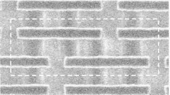
Intel reaches 45 nanometer chip milestone

Intel said Wednesday it had produced the semiconductor industry's first chip using milestone 45-nanometer process technology.
The Static Random Access Memory (SRAM) devices were produced using technology considered the next step forward in mass production of chips used in popular consumer high-tech devices.

Most current nano chip production is at the 65-nanometer level with the even-smaller 45-nanometer mark considered the next level.
Intel’s 45nm process technology will allow chips with more than five times less leakage power than those made today. This will improve battery life for mobile devices and increase opportunities for building smaller, more powerful platforms.
The 45nm SRAM chip has more than 1 billion transistors. Though not intended as an Intel product, the SRAM demonstrates technology performance, process yield and chip reliability prior to ramping processors and other logic chips using the 45nm manufacturing process. It is a key first step in the march toward high–volume manufacturing of the world’s most complex devices.
"Our 45nm technology will provide the foundation for delivering PCs with improved performance-per-watt that will enhance the user experience," promised Intel's Bill Holt.
The SRAMs were developed at Intel's Oregon facility. The company is establishing fabrication lines in Arizona and Israel to perform 45-nanometer mass production.
Copyright 2006 by United Press International


