How laser annealing technology can lead to production of ultrathin nanomaterials

Smart phones have shiny flat AMOLED displays. Behind each single pixel of these displays hide at least two silicon transistors which were mass-manufactured using laser annealing technologies. While the traditional methods to make them uses temperatures above 1,000 °C, the laser technique reaches the same results at low temperatures even on plastic substrates (melting temperature below 300 °C). Interestingly, a similar procedure can be used to generate crystals of graphene. Graphene is a strong and thin nano-material made of carbon, its electric and heat-conductive properties have attracted the attention of scientists worldwide.
Prof. KEON Jae Lee's research group at the Center for Multidimensional Carbon Materials (cmcm.ibs.re.kr/html/cmcm_en/) within the Institute for Basic Science (IBS) and Prof. CHOI Sung-Yool's team at KAIST discovered graphene synthesis mechanism using laser-induced solid-state phase separation of single-crystal silicon carbide (SiC). This study, available on Nature Communications, clarifies how this laser technology can separate a complex compound (SiC) into its ultrathin elements of carbon and silicon.
Although several fundamental studies understood the effect of excimer lasers in transforming elemental materials like silicon, the laser interaction with more complex compounds like SiC has rarely been studied due to the complexity of compound phase transition and ultra-short processing time.
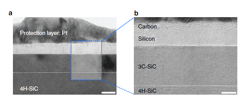
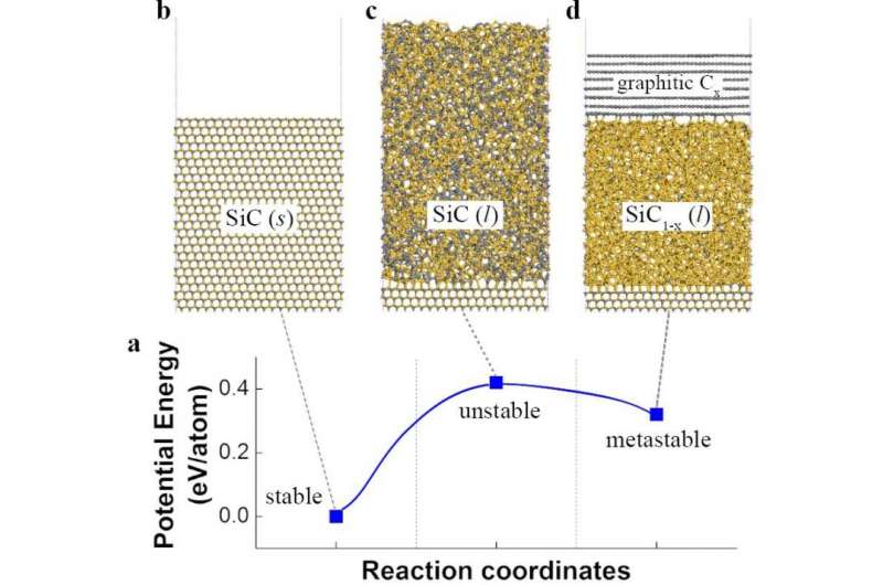
With high resolution microscope images and molecular dynamic simulations, scientists found that a single-pulse irradiation of xenon chloride excimer laser of 30 nanoseconds melts SiC, leading to the separation of a liquid SiC layer, a disordered carbon layer with graphitic domains (about 2.5 nm thick) on top surface and a polycrystalline silicon layer (about 5 nm) below carbon layer. Giving additional pulses causes the sublimation of the separated silicon, while the disordered carbon layer is transformed into a multilayer graphene.
"This research shows that the laser material interaction technology can be a powerful tool for next generation of two dimensional nanomaterials," said Prof. Keon. Prof. Choi added: "Using laser-induced phase separation of complex compounds, new types of two dimensional materials can be synthesized in the future." IBS Prof. Keon is affiliated with the School of Materials Science and Engineering, KAIST and Prof. Choi with the School of Electrical Engineering and Graphene Research Center, KAIST.

More information: Insung Choi et al. Laser-induced phase separation of silicon carbide, Nature Communications (2016). DOI: 10.1038/ncomms13562
Journal information: Nature Communications
Provided by Institute for Basic Science


