Interactions in designer materials unveiled

The fascinating properties of graphene—a single layer of carbon atoms—have been widely celebrated. Not only does graphene exhibit remarkable physics, it also shows great promise for new applications, like flexible display screens and solar cells. But scientists aren't easily satisfied. The hunt is on for the next generation materials—layered stacks composed of single sheets of 'flat' materials like boron nitride (BN), graphene (C) or tungsten disulfide (WS2).
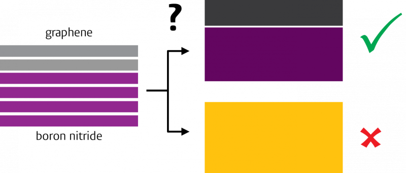
The trick is that such a layer cake is not just the sum of its parts. You might get properties completely different from those of the individual layers. This even goes for two layers of the same sort; bilayer graphene is in no way like its monolayer cousin. It all depends on how the layers interact. Leiden physicist Sense Jan van der Molen and his group have developed a method to determine the interaction between layers in each combination of materials.
LEEM
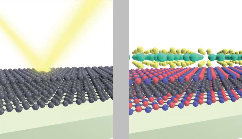
Using a technique called low-energy electron microscopy (LEEM), they shine electrons of very low energies at a sample. For every energy level, they record an image of the surface, telling them how many electrons are reflected. This gives them all the necessary information to determine the interlayer interaction and therefore the properties of the newly created material. Their method resolves details 100,000 times smaller than other techniques. This is crucial because novel nanomaterials are typically extremely small—less than the thickness of a human hair.
Tailored

'We used our method to prove that boron nitride and graphene do not interact with each other as was only assumed so far,' says first author and Veni fellow Johannes Jobst. 'But more importantly, it shows the potential of this novel technique. Now we can study any other combination of layers, like semiconductors on graphene, or two different semiconductors. And once we understand how this interaction works, we can freely design materials that are tailored to specific needs.'
More information: Johannes Jobst et al. Quantifying electronic band interactions in van der Waals materials using angle-resolved reflected-electron spectroscopy, Nature Communications (2016). DOI: 10.1038/ncomms13621
Journal information: Nature Communications
Provided by Leiden Institute of Physics


