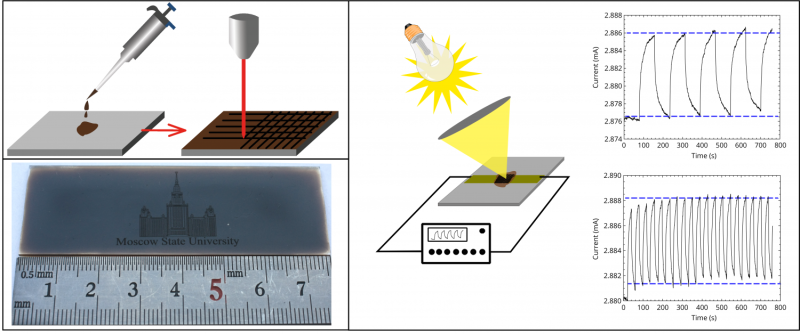
Prototype device for measuring graphene-based electromagnetic radiation

A prototype device called a bolometer measures electromagnetic radiation energy flow based on physical parameter variations of thermosensitive elements as a result of heating by absorption of radiation energy.
"We studied thermal and optical properties of the carbon structures derived from reduced graphene oxide in a wide range of wavelengths from visible to infrared. In addition to the optical and thermal properties of the carbon structures, we have demonstrated the bolometer prototype that operates at room temperature without additional cooling," says Stanislav Evlashin, the first author of the article, the researcher of the Skobeltsyn Institute of Nuclear Physics Lomonosov Moscow State University (SINP MSU), PhD in Physico-Mathematical Sciences.
Synthesis and investigations of the new materials for bolometric sensors have great scientific and practical importance. Such materials should possess a high effective absorption over a wide spectral range, high stable thermoresistive effect (change in electrical conductance with temperature), and they must be cheap to manufacture.
To create the bolometer prototype, the researchers used a water solution of graphene oxide, which was obtained by the widely used method of graphite oxidation. The resulting suspension of graphene oxide was deposited on the substrate for subsequent laser microstructuring. Laser treatment causes the partial reduction of graphene oxide film and changes the morphology. Consequently, it changes optical and thermal properties of graphene oxide.
The material synthesis for the bolometer prototype was developed at SINP MSU. Studies on the optical properties were carried out at the Physics Department of Moscow State University. Research on the thermal properties was carried out at LPI RAS.
"Laser microstructuring of graphene oxide opens the possibility of selective creation of antireflective, thermally conductive and electrically conductive coatings. The method is quite cheap, compatible with conventional semiconductor technology and produces antiabsorbing coatings that would cover large areas on almost any surface. The observed properties of reduced graphene oxide partially show the prospects of its use in bolometric matrices and other IR devices," says Stanislav Evlashin.
More information: Stanislav Evlashin et al, Controllable Laser Reduction of Graphene Oxide Films for Photoelectronic Applications, ACS Applied Materials & Interfaces (2016). DOI: 10.1021/acsami.6b10145
Journal information: ACS Applied Materials and Interfaces
Provided by Lomonosov Moscow State University


