New technique integrates graphene, graphene oxide and reduced graphene oxide onto silicon chips at room temperature

Materials researchers at North Carolina State University have developed a technique that allows them to integrate graphene, graphene oxide (GO) and reduced graphene oxide (rGO) onto silicon substrates at room temperature by using nanosecond pulsed laser annealing. The advance raises the possibility of creating new electronic devices, and the researchers are already planning to use the technique to create smart biomedical sensors.
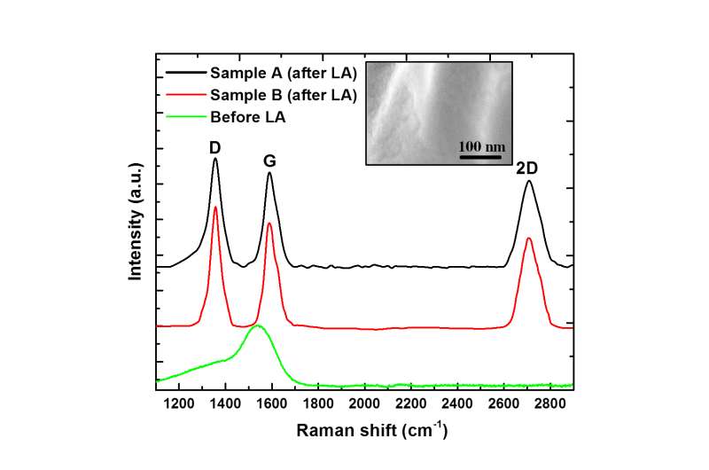
In the new technique, researchers start with a silicon substrate. They top that with a layer of single-crystal titanium nitride, using domain matching epitaxy to ensure the crystalline structure of the titanium nitride is aligned with the structure of the silicon. Researchers then place a layer of copper-carbon (Cu-2.0atomic percent C) alloy on top of the titanium nitride, again using domain matching epitaxy. Finally, the researchers melt the surface of the alloy with nanosecond laser pulses, which pulls carbon to the surface.
If the process is done in a vacuum, the carbon forms on the surface as graphene; if it is done in oxygen, it forms GO; and if done in a humid atmosphere followed by a vacuum, it forms as rGO. In all three cases, the carbon's crystalline structure is aligned with the underlying copper-carbon alloy.
"We can control whether the carbon forms one or two monolayers on the surface of the material by manipulating the intensity of the laser and the depth of the melting," says Jay Narayan, the John C. Fan Distinguished Chair Professor of Materials Science and Engineering at NC State and senior author of a paper describing the work.
"The process can easily be scaled up," Narayan says. "We've made wafers that are two inches square, and could easily make them much larger, using lasers with higher Hertz. And this is all done at room temperature, which drives down the cost."
Graphene is an excellent conductor, but it cannot be used as a semiconductor. However, rGO is a semiconductor material, which can be used to make electronic devices such as integrated smart sensors and optic-electronic devices.
"We have already patented the technique and are planning to use it to develop smart biomedical sensors integrated with computer chips," Narayan says.
The paper, "Wafer Scale Integration of Reduced Graphene Oxide by Novel Laser Processing at Room Temperature in Air," was published Sept. 9 in the Journal of Applied Physics.
More information: Anagh Bhaumik et al, Wafer scale integration of reduced graphene oxide by novel laser processing at room temperature in air, Journal of Applied Physics (2016). DOI: 10.1063/1.4962210
Journal information: Journal of Applied Physics
Provided by North Carolina State University


