September 5, 2016 feature
Cool Constructs: Room temperature out-of-plane ferroelectricity at ultrathin atomic limit

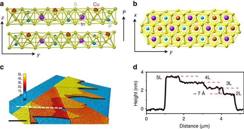
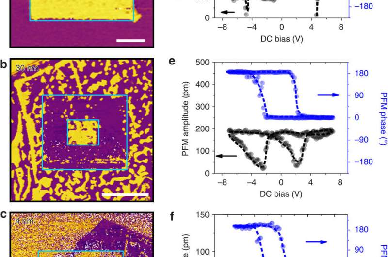
(Phys.org)—Optoelectronic devices that combine electronics and photonics are incorporating two-dimensional (2D) materials for a range of applications. At the same time, cooperative phenomena – in which a system's individual components appear to act as a single entity rather than independently – have yet to be widely investigated, an important example being ferroelectricity (spontaneous electric polarization that can be reversed by an electric field) in the 2D limit. Recently, however, scientists at Nanyang Technological University, Singapore have demonstrated room-temperature out-of-plane ferroelectricity (that is, orthogonal to the 2D material) in 2D CuInP2S6 (copper indium thiophosphate) with a ~320 K transition temperature, as well as switchable polarization in 4 nm CuInP2S6 flakes. The researchers state that their findings create the possibility of sensors, actuators, non-volatile memory devices, various van der Waals heterostructures (devices made from layers of dissimilar 2D crystals in which forces are based on molecular attraction or repulsion rather than covalent or ionic bonds), and other novel applications based on 2D ferroelectricity.
Prof. Zheng Liu and Prof. Junling Wang discussed the challenges that they and their colleagues encountered in conducting their study published in Nature Communications. "With reduced dimension, ferroelectricity – namely, long-range electric-dipole order – becomes fragile owing to the depolarization field that is opposing its own electric polarization," Liu tells Phys.org. "The depolarization field inherently arises in ferroelectric materials due to the imperfect screening of bound charges," that is, those bound to molecules and so cannot move in response to an external electromagnetic force. The difficulty lies in maintaining a precise geometry, Liu adds, because when the ferroelectric material's thickness is reduced to its two-dimensional limit, the depolarization field can increase by orders of magnitude. At that point, the depolarization field may place the ferroelectric material into a paraelectric state, the result being disordered electric dipoles with a temporary polarization only when in the presence of an electric field. Therefore, the electrical boundary conditions are extremely important when exploring ferroelectricity at the material's 2D limit. Moreover, he adds, reporting the experimental observation of switchable polarization in CuInP2S6 films down to 4 nm at room temperature, thickness reduction will greatly weaken the out-of-plane ferroelectric polarization. "This makes characterization of the ferroelectricity very difficult. Moreover, the large ionic conductivity of this material makes the polarization switching quite challenging. We therefore had to choose a small electric field that is just above the coercive field to avoid unwanted ionic motion."
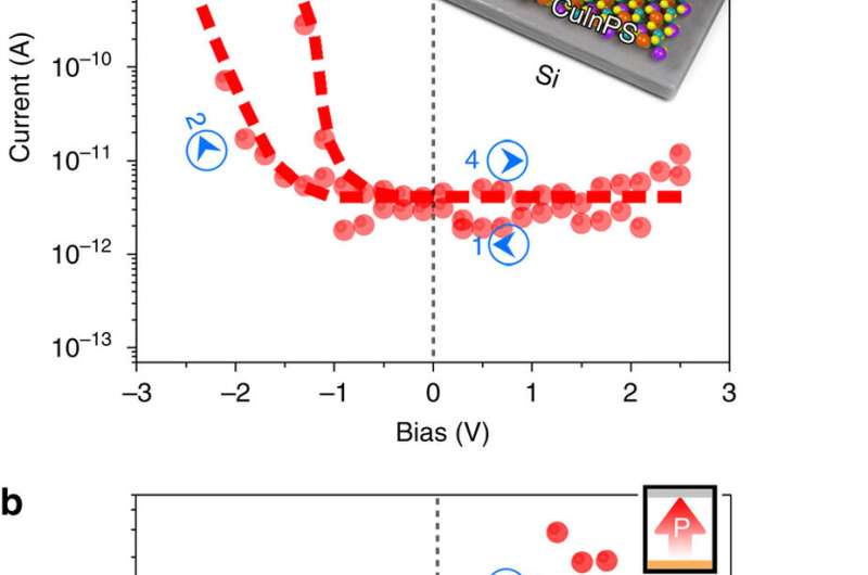
Other concerns include demonstrating the potential of this 2D ferroelectric material by preparing a van der Waals ferroelectric diode formed by CuInP2S6/Si heterostructure. "In the case of CuInP2S6, the chemical composition and phase stability also play a role in stabilizing ferroelectric states – and in the 2D limit, it is difficult to determine the ferroelectricity with traditional methods, such as the time-dependent ferroelectric hysteresis loop measurement, due to large leakage current," lead author Liu Fucai points out. Regarding potential, he explains that due to the relatively large band gap and thus weak light absorption, few-layer CuInP2S6 appears almost transparent on silicon (Si) substrate. "This situation makes the fabrication of the van der Waals heterostructure quite challenging during the lithography process."

Finally, in demonstrating a non-volatile memory device with an on/off ratio of ~100 in a CuInP2S6/Si ferroelectric diode, Liu notes that this investigation is just a preliminary demonstration of the possible applications of the 2D ferroelectric material. "A lot of work needs to be done to fully understand the transport mechanisms and how it is coupled to the ferroelectric switching," he acknowledges.
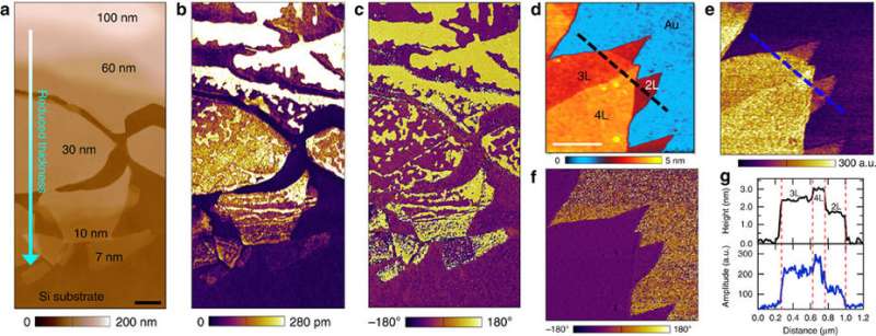
Wang describes the ways in which the researchers addressed these challenges. "To characterize ferroelectricity at nanoscale, the most widely used technique is called piezoresponse force microscopy, or PFM, which utilizes the converse piezoelectric effect." (In the converse piezoelectric effect, materials become strained when an electric field is applied.) This is a technique that can be implemented using a commercially available atomic force microscope (AFM), in which AC bias can be applied to the AFM probe that serves as a moving electrode on top of the sample. The resulting AC electric field will cause the periodic oscillation of the ferroelectric sample due to this converse piezoelectric effect. The oscillation signal can then be detected by the AFM.
"The amplitude of the oscillation represents the piezoelectric response that is proportional to the ferroelectric polarization," Wang explains, "while the phase of the oscillation represents the direction of the polarization." In their study, the scientists employed a state-of-the-art approach known as Dual AC Resonance Tracking (DART) PFM developed by Asylum Research to amplify the piezoelectric response by taking advantage of the resonance enhancement.

"By driving the AC field at the first harmonic contact resonance," Wang continues, "the piezoelectric oscillation signal can be greatly enhanced. Thus, the small ferroelectric polarization of the ultrathin CuInP2S6 flakes can still be detected by the AFM, as the signal has been amplified by orders of magnitude. This advanced PFM technique helps us to image the fine domain structure with nanometer lateral resolution and picometer vertical resolution, and thereby realize local ferroelectric switching using an AFM probe."
The paper discusses novel applications, including sensors, actuators, non-volatile memory devices, and various van der Waals heterostructures based on 2D ferroelectricity. "By virtue of the piezoelectric effect, ferroelectric materials always have the piezoelectric and pyroelectric properties that allow the use of atomically-thin CuInP2S6 as a strain sensor with high flexibility, such as electric skin monitoring human body motion," Liu tells Phys.org. "By using the pyroelectric effect, 2D CuInP2S6 could also be used for thermal energy harvesting, and as we know, commercially available ferroelectric random access memory, or FeRAM" – random-access memory similar to DRAM – "with fast writing speed and low-power consumption, but with destructive readout could be improved by employing a ferroelectric diode to achieve non-destructive readout of the information. Considering the quasi-freestanding nature of 2D materials, ferroelectric diodes, or even ferroelectric tunnel junctions with an atomically thin ferroelectric layer may have a much higher ON/OFF ratio, providing the possibility of high-density ferroelectric memories with non-destructive readout."
Regarding the relationship between, and potential applications deriving from, ferro- and piezoelectric effects and van der Waals heterostructure interactions, Liu notes that vertically stacking of different 2D materials with van der Waals force have revealed unusual properties and have been investigated for the application of tunneling transistors, light emitting diodes, and light harvesting devices. "Incorporating ferroelectricity to the van der Waals heterostructure could demonstrate new functionality, such as ferroelectric field transistors and optoelectronic memory, by combining CuInP2S6 with 2D semiconductors."

The scientists are planning to study the pyroelectric properties of CuInP2S6 at its two-dimensional limit and apply their findings to developing energy harvesting devices. To that end, he adds, because mechanically exfoliated 2D materials are usually small and unsuitable for device applications, chemical vapor deposition growth of atomically thin CuInP2S6 is under development.
"Ferroelectric properties are also very interesting for solar cell applications because of efficient ferroelectric polarization-driven carrier separation," Liu concludes, "so 2D ferroelectricity-based solar cells could be very interesting, In its liquid phase, 2D ferroelectric CuInP2S6 could be easily hybridized with semiconductor 2D or organic materials – and a solar cell based on these hybrids would be very promising."
More information: Room-temperature ferroelectricity in CuInP2S6 ultrathin flakes, Nature Communications 7, Article number: 12357 (2016), doi:10.1038/ncomms12357
Related:
1. Subatomic deformation driven by vertical piezoelectricity from CdS ultrathin films, Science Advances 01 Jul 2016, Vol. 2, no. 7, e1600209, doi:10.1126/sciadv.1600209
2. Picoscale precision though ultrathin film piezoelectricity, Phys.org (10 August 2016), http://phys.org/news/2016-08-picoscale-precision-ultrathin-piezoelectricity.html
Journal information: Nature Communications , Science Advances
© 2016 Phys.org


